
Printed circuit board and method for manufacturing the same

a printed circuit board and manufacturing method technology, applied in the direction of printed circuit manufacturing, printed circuit aspects, metallic pattern materials, etc., can solve the problems of interlayer adhesion and appearance of the final product, the peel strength of the black oxide treatment method is about 0.2 kgf/cm, and the peel strength is not suitable for a high reliability product requiring a peel strength of at least 0.4 kgf. , to achieve the effect of improving the interlayer adhesion of the pcb

Active Publication Date: 2015-12-31
SAMSUNG ELECTRO MECHANICS CO LTD
View PDF2 Cites 6 Cited by
  • Summary
  • Abstract
  • Description
  • Claims
  • Application Information

AI Technical Summary

Benefits of technology

The method significantly improves interlayer adhesion with prepregs, particularly with BT resin, while minimizing roll marks and maintaining acid resistance, thus enhancing the reliability and appearance of PCBs, and reducing production time and costs.

Problems solved by technology

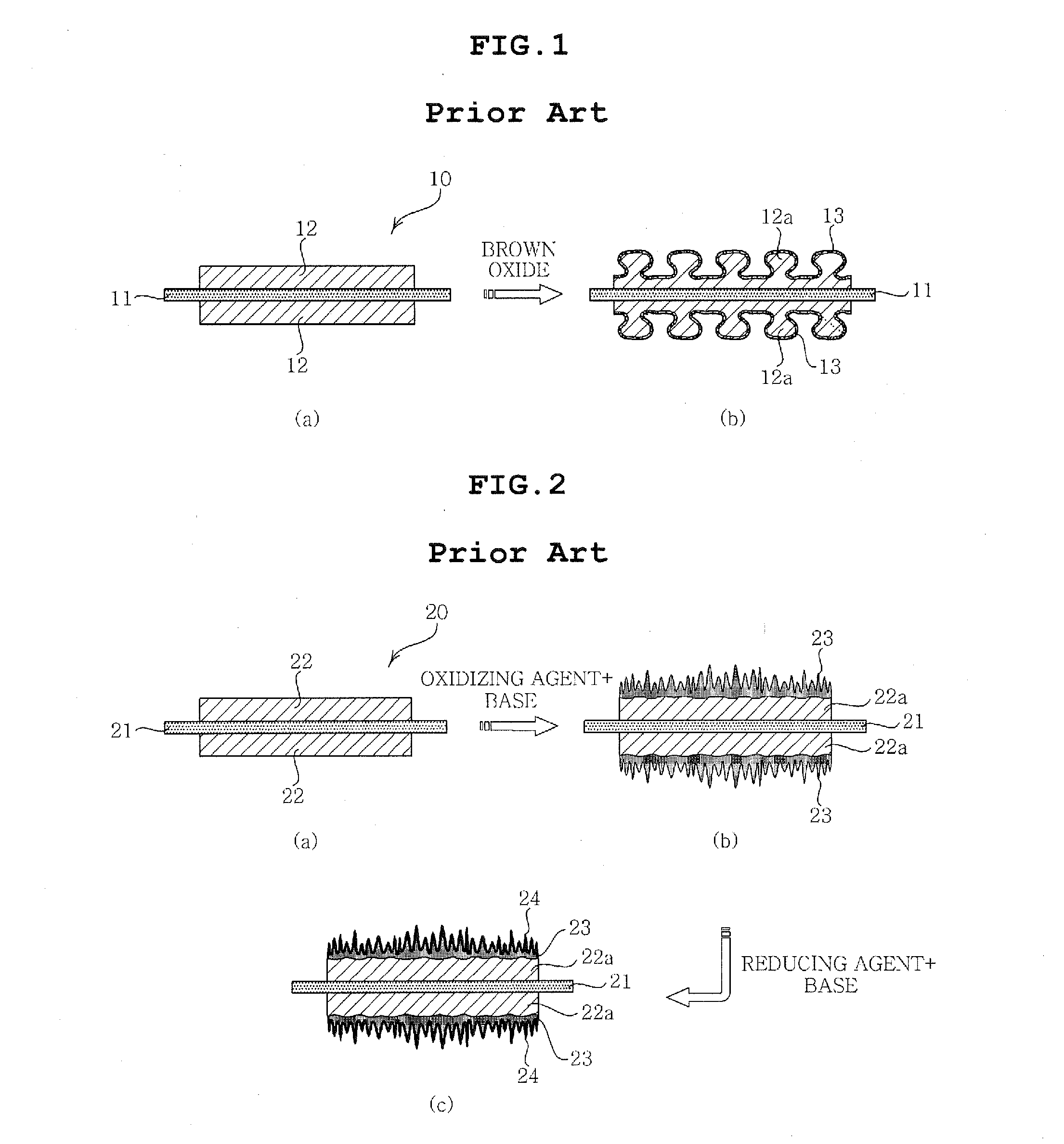
For instance, when a bismaleidotriazine (BT) resin having a Tg of more than 200° C., excellent characteristics such as heat resistance, dielectric properties, insulating properties and / or migration-resistance, and favorable activity under molding conditions is used as a prepreg for manufacturing a semiconductor packaging substrate, the substrate treated by a conventional brown oxide treatment or black oxide treatment method has a peel strength of about 0.2 kgf / cm, which is not suitable for a high reliability product requiring a peel strength of at least 0.4 kgf / cm.
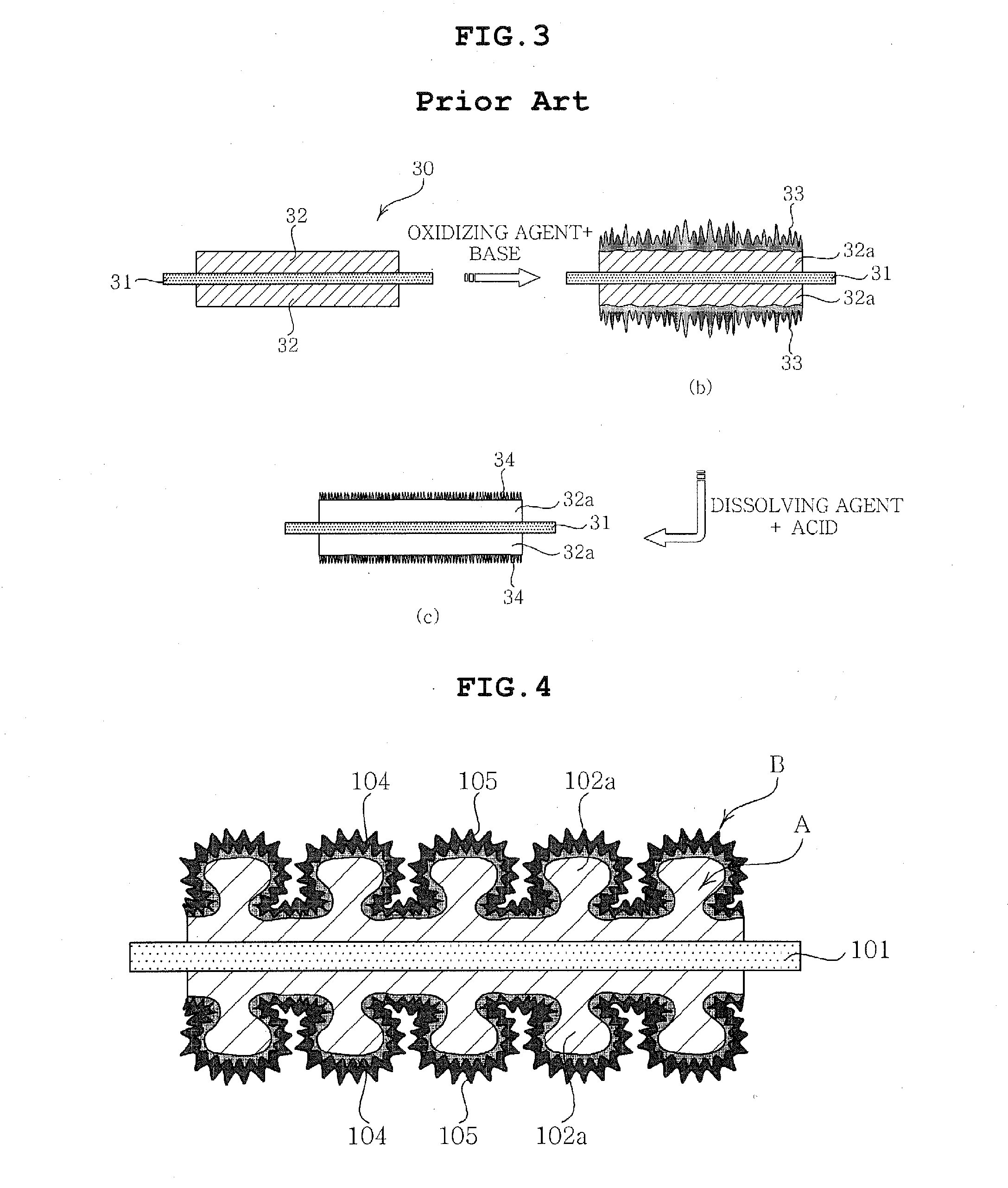
In particular, if a black-oxide treatment process is conducted in a horizontal roll type line, a substrate may have numerous roll marks generated on a surface thereof, which in turn causes Cu exposure, thus causing problems in interlayer adhesion and appearance of a final product.

Method used


Image

  • Printed circuit board and method for manufacturing the same
  • Printed circuit board and method for manufacturing the same
  • Printed circuit board and method for manufacturing the same

Examples


example 1

[0147]According to a process sequence illustrated in FIG. 6, surface treatment of a circuit metal for a PCB was performed.

[0148]A degreasing process was conducted by treating a test specimen made of a copper clad laminate (CCL; 406 mm×510 mm, 0.1 mm in thickness) and a copper foil (330 mm×400 mm, 35 μm in thickness) using a solution of 20 wt. % MC100 (KENSCO Co., a basic cleaner) in deionized water at 60° C. for 1 minute and then washing the same.

[0149]After the degreasing process, an etching process was conducted by treating the test substrate, that is, the specimen (made of CCL and Cu foil) in an etching solution comprising 12 wt. % of sodium persulfate, 5 wt. % of sulfuric acid and 15 wt. % of BF200A (KENSCO Co., a roughness forming etchant) and the remainder of deionized water at room temperature for 1 minutes and then washing the same.

[0150]After the etching process, a pre-dipping process was conducted by treating the etched specimen using a solution of 30 wt. % BF300A (KENSCO ...

example 2

[0153]The present experiment was substantially performed according to the same procedures as described in Example 1, except that the post-dipping solution used herein was a dissolving solution comprising 40 wt. % of HR400A (KENSCO Co., a dissolving agent) and 10 wt. % of HR400B (KENSCO Co., a dissolving agent) in deionized water and the post-dipping process was conducted at 45° C. for 1 minute.

[0154]The black oxide layer of the specimen prepared according to the foregoing example had an average film thickness of 0.1 to 0.6 mg / cm2.

experimental example

[0156]For assessment of reliability, a CCL specimen (406 mm×510 mm) with a predetermined thickness was firstly prepared, and weighed before and after formation of a black oxide layer thereon. Then, a difference in measured weights of the specimen was calculated to estimate a thickness of the black oxide layer. Alternatively, for determination of an etching rate, the CCL specimen (100 mm×100 mm) was cut into pieces having a predetermined size and each cut piece was weighed before and after the etching process. Then, a difference in measured weights of the specimen was calculated to determine the etching rate. For the inventive example, the thickness of the black oxide layer was constantly maintained in the range from 0.8 to 1.2 μm. Furthermore, interlayer adhesion between the Cu foil and resin was assessed by the following procedures. According to assessment items and procedures listed in Table 1, a prepreg (BT resin, GHPL-830, Tg=215° C.) and the treated Cu foil specimen (300 mm×400...


PUM


Abstract

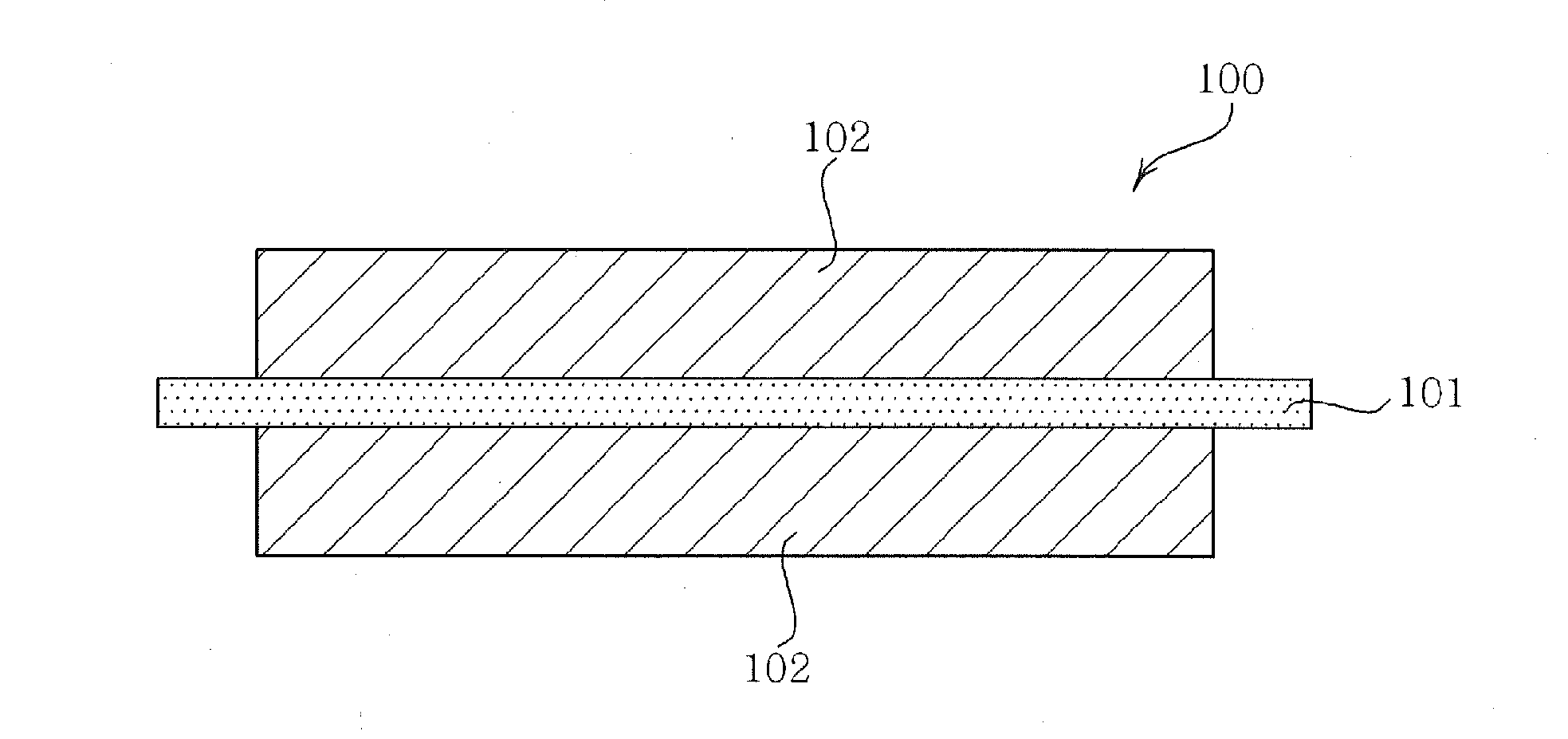
Disclosed herein are a printed circuit board and a method for manufacturing the same. The printed circuit board includes: a base substrate having a metal pattern for a circuit; and a surface roughness provided on the metal pattern, wherein the surface roughness has a first surface roughness in an anchor structure and a second surface roughness having a black oxide layer in a needle structure formed on the first surface roughness.

Description

CROSS REFERENCE TO RELATED APPLICATION[0001]This application is a Divisional application of U.S. application Ser. No. 13 / 308,439, filed Nov. 30, 2011, which claims the benefit under 35 U.S.C. §119(a) of Korean Patent Application No. 10-2010-0138241, filed Dec. 29, 2010, in the Korean Intellectual Property Office, the disclosures of both of which are incorporated herein by reference for all purposes.BACKGROUND OF THE INVENTION[0002]1. Technical Field[0003]The present invention relates to a printed circuit board and a method for manufacturing the same.[0004]2. Description of the Related Art[0005]Technical development for size and weight reduction, and thinner and simpler configuration of an electronic apparatus such as a laptop computer, a net-book, a tablet PC, a smart phone, a navigator, and the like has remarkably increased. Technologies for size and weight reduction, and thinner and simpler configuration of an electronic apparatus require not only techniques of decreasing the size...

Claims


Application Information

Patent Timeline
Patent Type & Authority Applications(United States)
IPC IPC(8): H05K1/09
CPCH05K3/383H05K3/385H05K3/462H05K1/11H05K1/0284H05K1/09H05K2201/0239H05K2201/0195
Inventor HA, HYUNG GIJUNG, JAE WONKIM, YONG HWANLEE, JONG JINKOO, JA HOSHIN, YOUNG HWANLEE, DONG KYU
Owner SAMSUNG ELECTRO MECHANICS CO LTD
Learn More