Fault tolerant design for large area nitride semiconductor devices

a technology of nitride semiconductors and fault tolerance, which is applied in the direction of semiconductor devices, semiconductor/solid-state device testing/measurement, semiconductor/solid-state device details, etc., can solve the problems of increasing the probability of one or more faults or defects, failure of the entire device, and complex and time-consuming electrical testing of each element separately, so as to facilitate electrical testing and defect isolation, improve fault tolerance

Active Publication Date: 2015-06-11
GAN SYST
View PDF1 Cites 11 Cited by
  • Summary
  • Abstract
  • Description
  • Claims
  • Application Information

AI Technical Summary

Benefits of technology

[0013]Thus, aspects of the invention provide systems and devices based on an island topology that provide improved fault tolerance and / or facilitate electrical testing and defect isolation.

Problems solved by technology

A fault in the active channel region of a conventional large gate width, multi-finger GaN transistor design, such as shown in FIG. 1B, can cause failure of the entire device.
As the device area increases, and depending on the defect density in active regions of the GaN semiconductor layer, the probability of one or more faults or defects increases.
Moreover, for large gate width transistors using a large number of island electrodes, it will be apparent that it becomes complex and time consuming to electrically test each element separately, i.e., to electrically test each source island, drain island and gate electrode combination, to find defective elements or defective areas of the semiconductor layer.

Method used


Image

  • Fault tolerant design for large area nitride semiconductor devices
  • Fault tolerant design for large area nitride semiconductor devices
  • Fault tolerant design for large area nitride semiconductor devices

Examples


Embodiment Construction

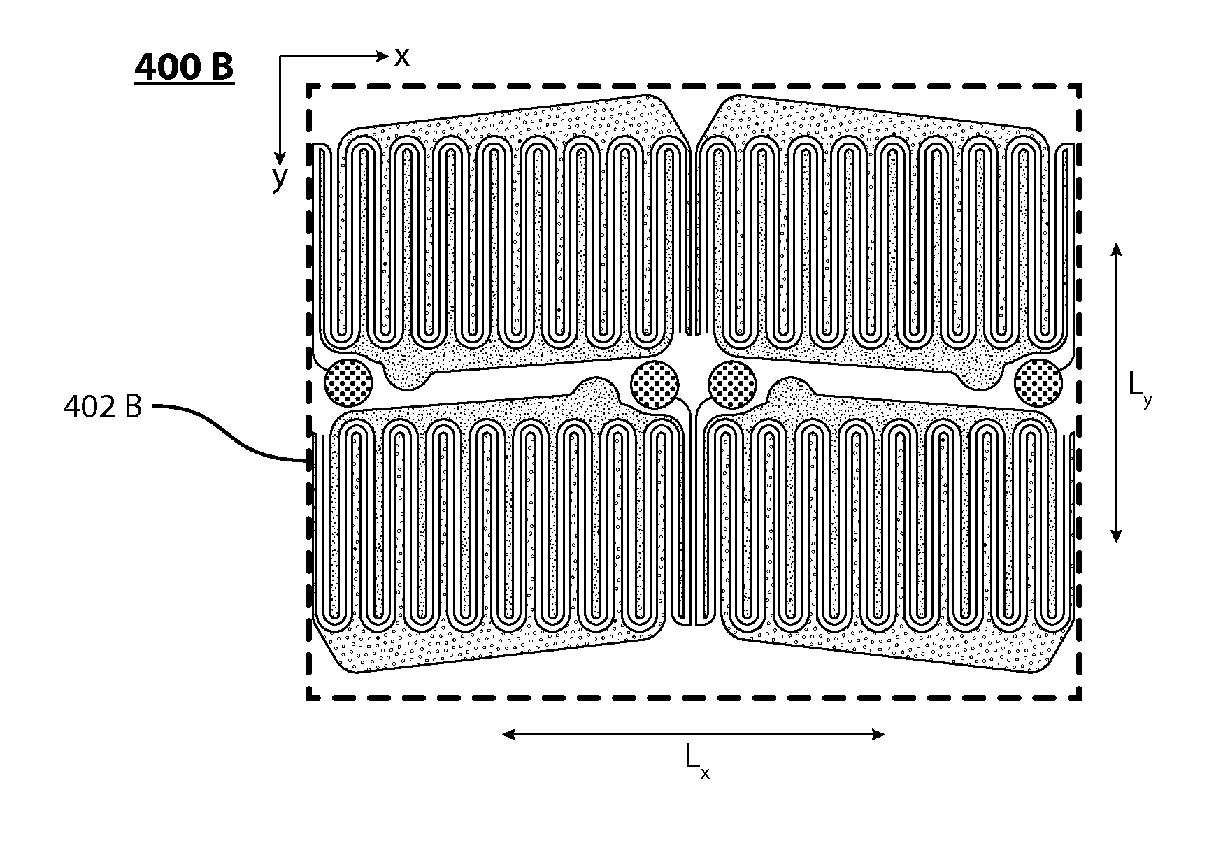
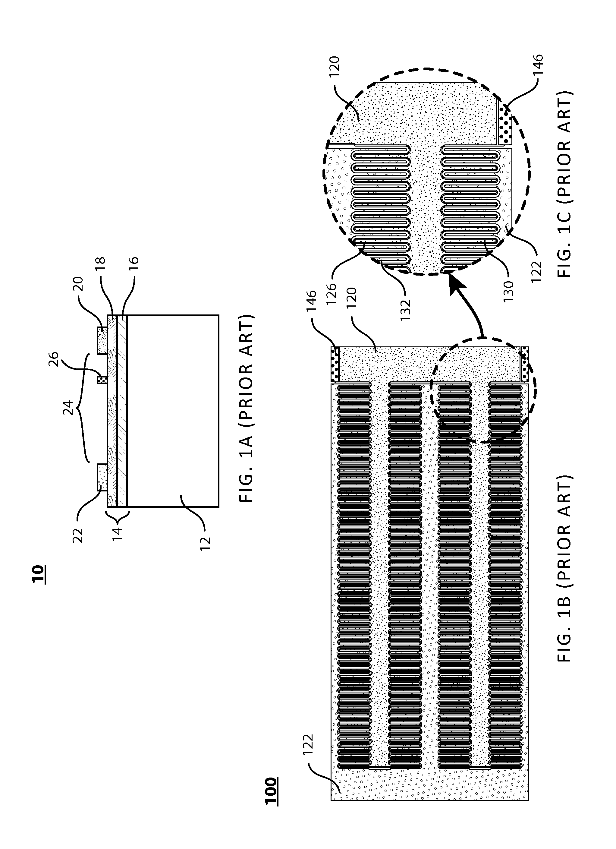
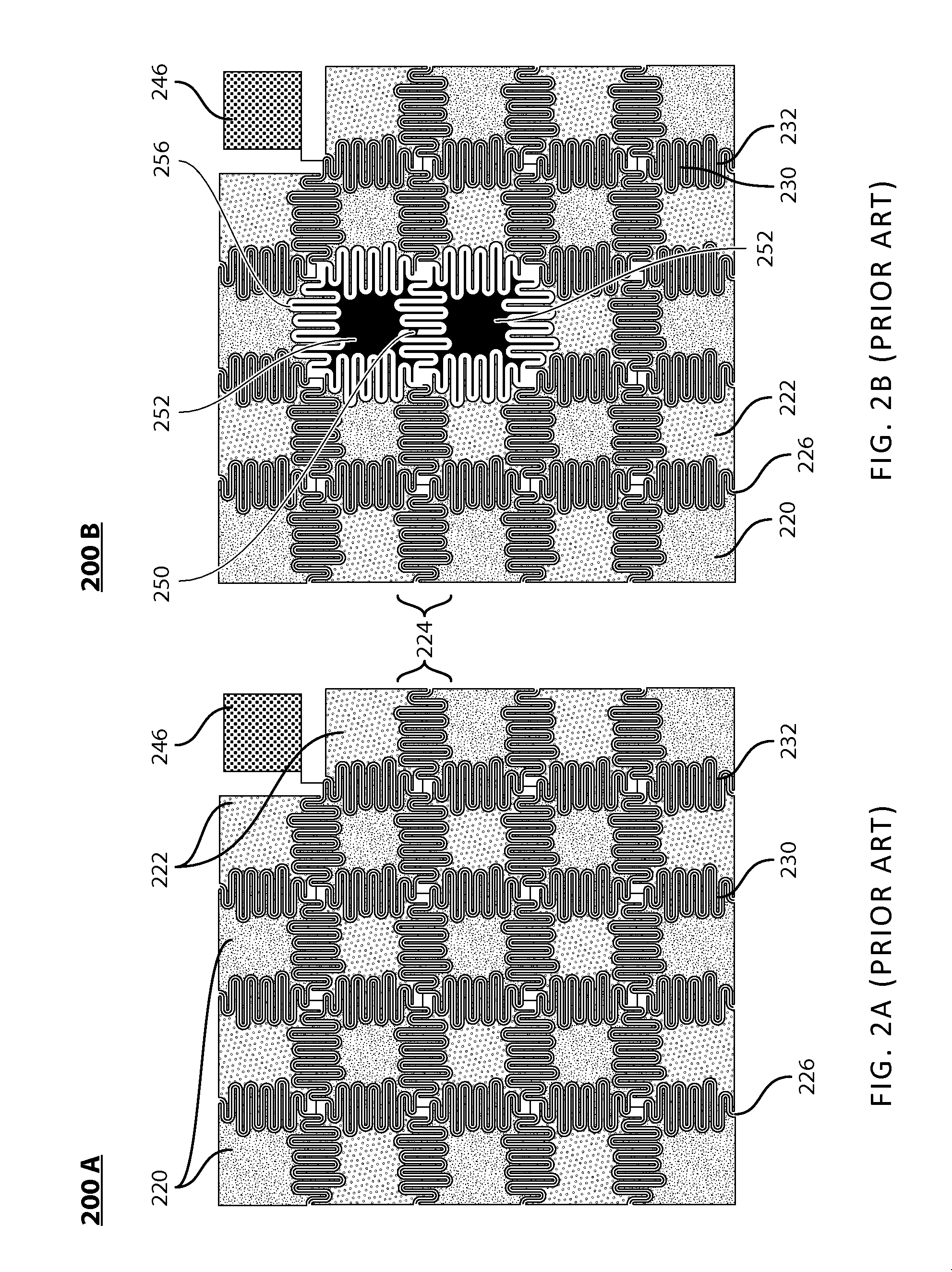
[0077]FIG. 1A shows a schematic diagram of a simple GaN transistor 10. The GaN power transistor 10 comprises a substrate 12, e.g., a silicon or silicon carbide wafer, on which an active GaN semiconductor layer 14 is formed. The GaN semiconductor layer 14 comprises, for example, a GaN / AlGaN hetero-structure layer, i.e., a layer of GaN 16 and an overlying layer of AlGaN 18 to form an active region comprising a two dimensional electron gas (2DEG). A source electrode 20 and a drain electrode 22 are provided on the active GaN semiconductor layer 14 to define a channel region 24 in the semiconductor layer between the source and drain electrodes, and a gate electrode 26 is provided over the channel region. In subsequent Figures, similar reference numerals, incremented by 100 in each successive figure, will be used to refer to these elements of each GaN transistor.

[0078]In practice, to provide a large area GaN power transistor with a large gate width Wg, e.g., for use in high voltage and hi...


PUM

PropertyMeasurementUnit
breakdown voltageaaaaaaaaaa
gate widthaaaaaaaaaa
areaaaaaaaaaaa

Abstract

A fault tolerant design for large area nitride semiconductor devices is provided, which facilitates testing and isolation of defective areas. A transistor comprises an array of a plurality of islands, each island comprising an active region, source and drain electrodes, and a gate electrode. Electrodes of each island are electrically isolated from electrodes of neighboring islands in at least one direction of the array. Source, drain and gate contact pads are provided to enable electrical testing of each island. After electrical testing of islands to identify defective islands, overlying electrical connections are formed to interconnect source electrodes in parallel, drain electrodes in parallel, and to interconnect gate electrodes to form a common gate electrode of large gate width Wg. Interconnections are provided selectively to good islands, while electrically isolating defective islands. This approach makes it economically feasible to fabricate large area GaN devices, including hybrid devices.

Description

CROSS-REFERENCE TO RELATED APPLICATIONS[0001]This application is a continuation of PCT International patent application no PCT / CA2014 / 000762, entitled “Fault Tolerant Design for Large Area Nitride Semiconductor Devices”, filed Oct. 28, 2014, designating the United States, and claiming priority from U.S. provisional patent application No. 61 / 896,871, entitled “Fault Tolerant Design for Large Area Nitride Semiconductor Devices” filed Oct. 29, 2013, both of which are incorporated herein by reference in their entirety.[0002]This application is related to: U.S. patent application Ser. No. 13 / 388,694, entitled “Island matrixed gallium nitride microwave and power switching transistors”, which is a national entry of PCT International application no. PCT / CA2010 / 001202, filed Aug. 4, 2010, designating the United States, and which claims priority from U.S. provisional patent application No. 61 / 231,139, filed Aug. 4, 2009; U.S. patent application Ser. No. 13 / 641,003, entitled “High density gall...

Claims


Application Information

Patent Timeline
Patent Type & Authority Applications(United States)
IPC IPC(8): H01L21/66H01L29/201H01L23/528H01L29/778H01L27/095H01L29/20H01L29/205
CPCH01L22/32H01L29/2003H01L29/201H01L23/528H01L29/7787H01L27/095H01L29/205H01L29/41758H01L29/42316H01L29/7786H01L23/4824H01L2924/0002H01L22/14H01L22/22H01L2924/00H01L29/0649H01L29/0657H01L29/1608H01L29/861
Inventor KLOWAK, GREGORY P.MCKNIGHT-MACNEIL, CAMERONTWEDDLE, HOWARDMIZAN, AHMADSPRINGETT, NIGEL
Owner GAN SYST
Why Eureka
Try Eureka