Methods of forming semiconductor structures
a technology of semiconductor structure and semiconductor substrate, which is applied in the direction of semiconductor device details, semiconductor/solid-state device devices, electrical equipment, etc., can solve the problems of reducing the performance of devices fabricated thereon, and reducing the efficiency of bulk silicon substrate removal
- Summary
- Abstract
- Description
- Claims
- Application Information
AI Technical Summary
Benefits of technology
Problems solved by technology
Method used
Image

Examples
Embodiment Construction
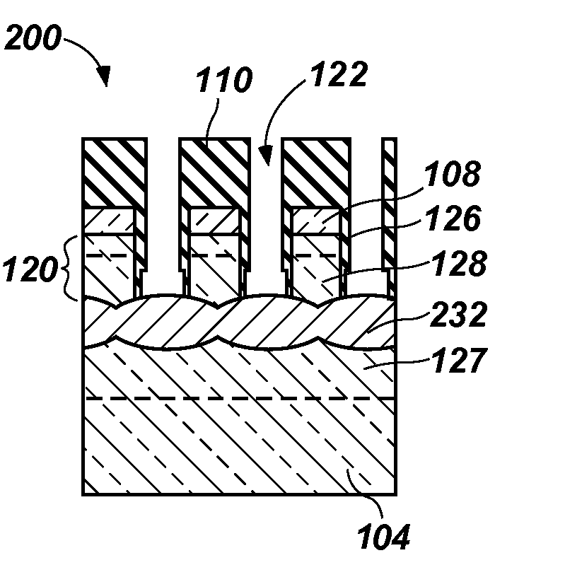
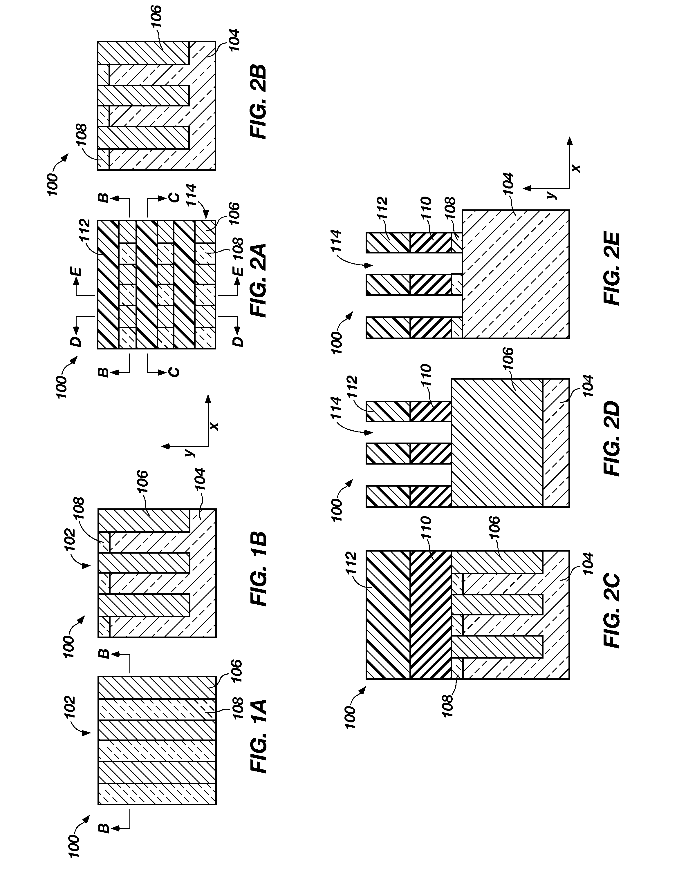
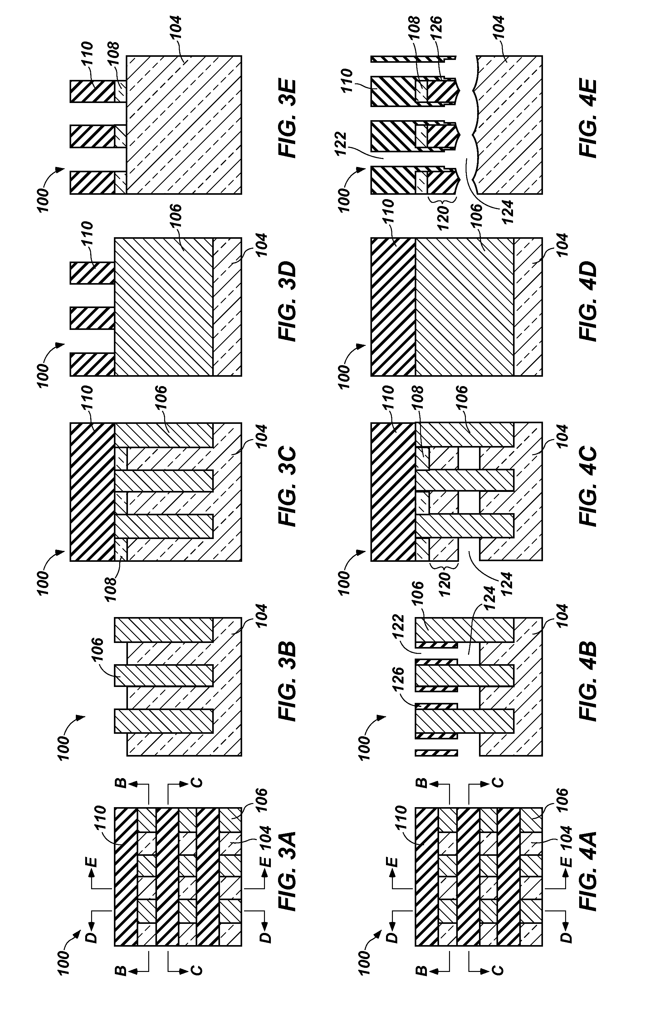
[0011]Methods of forming semiconductor structures are disclosed, as are semiconductor structures that include a conductive material underlying bodies of a semiconductor material. As used herein, the term “body” means and includes a volume of a semiconductor material. The bodies may be formed having a plurality of rails of a dielectric material between which the bodies of the semiconductor material are suspended. As used herein, the term “rails” means and includes a body of material having a substantially elongated shape, which may be used as a support for the bodies of semiconductor material. The conductive material, such as a metal, may be used as an interconnect structure to electrically couple components of memory devices. By way of example and not limitation, the conductive material may be used as a conductive line to electrically interconnect diode structures of a phase-change memory (PCRAM) device. As another example, the conductive material may be used as a buried strap to el...
PUM
| Property | Measurement | Unit |
|---|---|---|
| aspect ratio | aaaaa | aaaaa |
| temperature | aaaaa | aaaaa |
| semiconductor structure | aaaaa | aaaaa |
Abstract
Description
Claims
Application Information
 - R&D
- Intellectual Property
- Life Sciences
- Materials
- Tech Scout
- Unparalleled Data Quality
- Higher Quality Content
- 60% Fewer Hallucinations
Browse by: Latest US Patents, China's latest patents, Technical Efficacy Thesaurus, Application Domain, Technology Topic, Popular Technical Reports.
© 2025 PatSnap. All rights reserved.Legal|Privacy policy|Modern Slavery Act Transparency Statement|Sitemap|About US| Contact US: help@patsnap.com