Graded hardmask interlayer for enhanced extreme ultraviolet performance

a technology of extreme ultraviolet performance and hardmask, which is applied in the field of semiconductor processing, can solve problems such as resist scumming, and achieve the effect of reducing scumming defectivity and reducing scumming defectivity

Active Publication Date: 2021-05-04
INT BUSINESS MASCH CORP
View PDF17 Cites 2 Cited by
  • Summary
  • Abstract
  • Description
  • Claims
  • Application Information

AI Technical Summary

Benefits of technology

[0004]In accordance with another embodiment of the present invention, a method for semiconductor processing is provided. The method includes grading a hardmask, including a first material and a second material with high extreme ultraviolet (EUV) absorption cross sections for absorption of EUV wavelengths, by adjusting a percentage of the second material in the hardmask to include a highest percentage of the second material at a top surface of the hardmask. The method also includes depositing a photoresist layer over the hardmask. The method additionally includes patterning the photoresist layer with a dosage extreme ultraviolet source to reduce scumming defectivity. The method further includes etching the hardmask. The method also includes removing the photoresist layer.
[0005]In accordance with yet another embodiment of the present invention, a method for semiconductor processing is provided. The method includes grading a hardmask, including a first material and a second material with high extreme ultraviolet (EUV) absorption cross sections for absorption of EUV wavelengths, by adjusting a concentration of the second material in the hardmask by doping the first material with the second material. The method also includes depositing a photoresist layer over the hardmask. The method additionally includes patterning the photoresist layer with a dosage extreme ultraviolet source to reduce scumming defectivity. The method further includes etching the hardmask. The method also includes removing the photoresist layer.

Problems solved by technology

The resist thickness and / or exposure time along with development can cause resist scumming, which occurs when the resist is not sufficiently cleared.

Method used


Image

  • Graded hardmask interlayer for enhanced extreme ultraviolet performance
  • Graded hardmask interlayer for enhanced extreme ultraviolet performance
  • Graded hardmask interlayer for enhanced extreme ultraviolet performance

Examples


Embodiment Construction

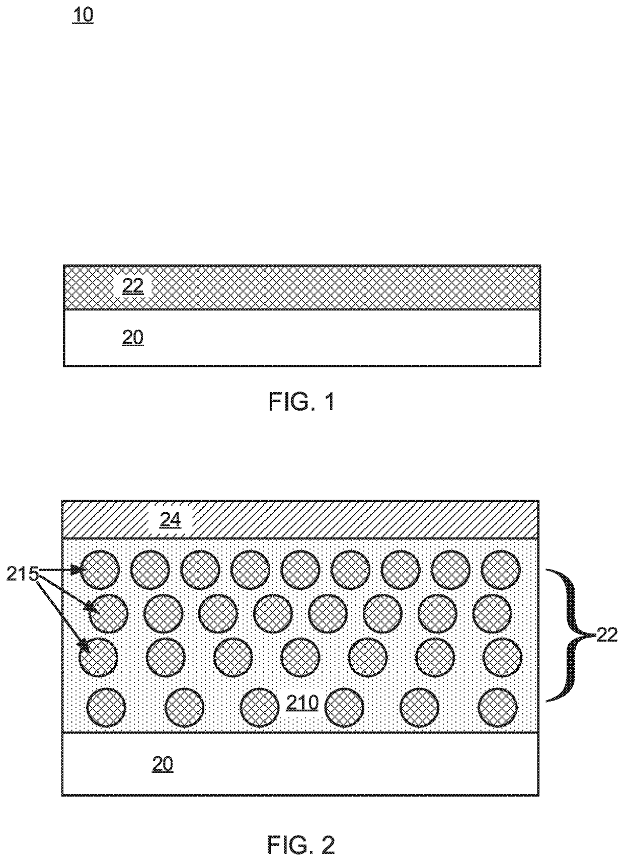
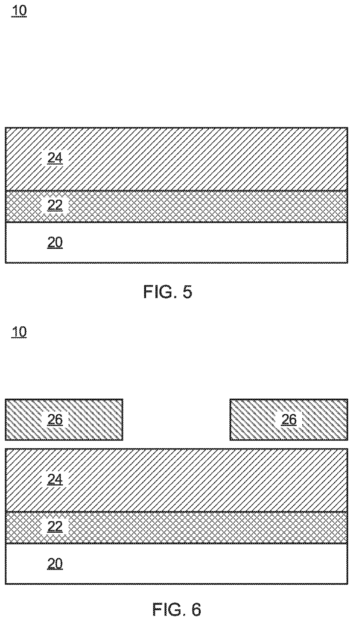
[0023]In accordance with aspects of the present invention, protective structures and processing methods are provided for processing semiconductor devices. In particularly useful embodiments, the processing methods can be employed in complementary metal oxide semiconductor (CMOS) device processing, especially where different areas of the CMOS device need to be protected during the CMOS forming process.

[0024]The semiconductor device can include a substrate. The substrate can include any structures formed therein. In one embodiment, the substrate can include an organic layer. The organic layer can include a single layer of organic material. The organic layer can also include a composite organic layer including a stack of organic and inorganic layers.

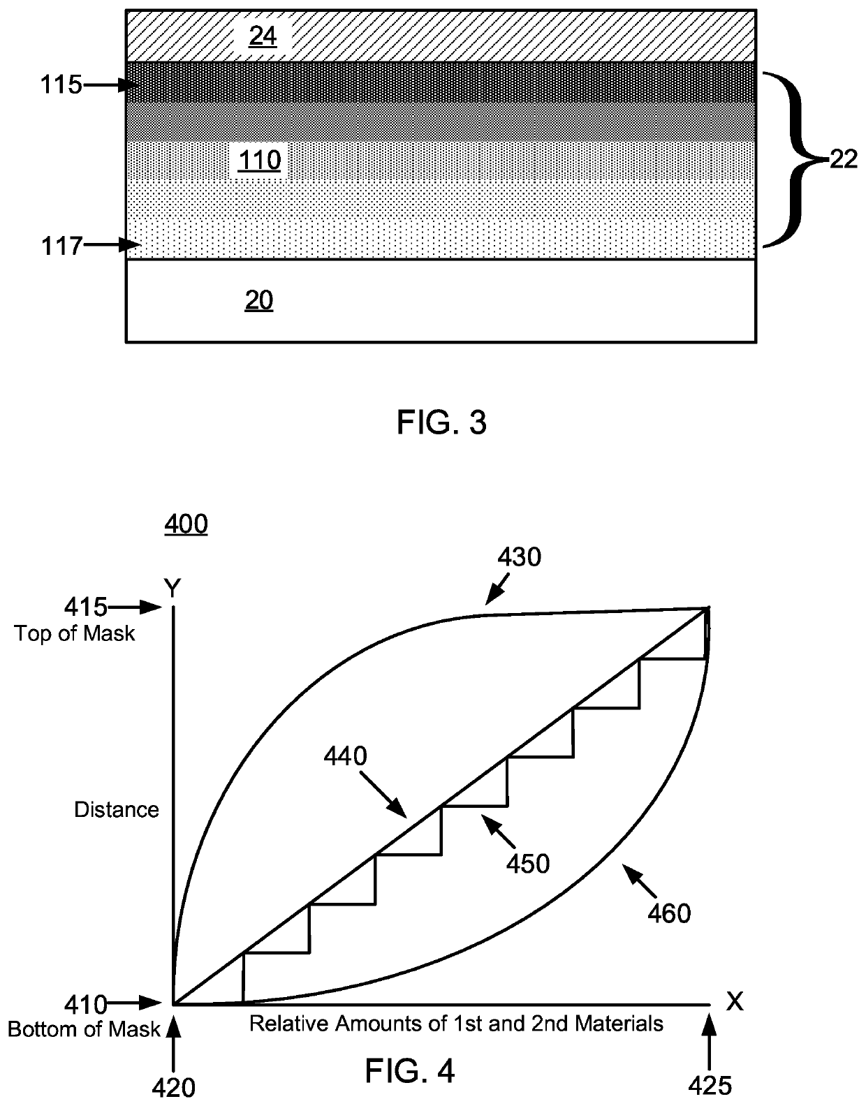
[0025]The semiconductor device can include a graded hardmask and a photoresist layer. Once the photoresist layer is applied to the semiconductor device, extreme ultraviolet (EUV) light lithography can be performed to pattern the photoresist...


PUM

PropertyMeasurementUnit
thicknessaaaaaaaaaa
sizesaaaaaaaaaa
sizesaaaaaaaaaa

Abstract

A patterning stack and methods are provided for semiconductor processing. The method includes forming a graded hardmask, the graded hardmask including a first material and a second material with extreme ultraviolet (EUV) absorption cross sections for absorption of EUV wavelengths, the second material configured to provide adhesion to photoresist materials. The method also includes depositing a photoresist layer over the graded hardmask. The method additionally includes patterning the photoresist layer. The method further includes etching the graded hardmask. The method also includes removing the photoresist layer.

Description

BACKGROUNDTechnical Field[0001]The present invention generally relates to semiconductor processing, and more particularly to a graded hardmask interlayer for enhancing extreme ultraviolet performance.Description of the Related Art[0002]Semiconductor patterning often employs masks for processing semiconductor structures. In some instances, multiple masking layers are employed to process different areas of a chip or wafer using different portions of the multilayered structure. In one example, patterning schemes can be employed utilizing a resist layer and photolithography to protect portions of the chip, etc. The resist thickness and / or exposure time along with development can cause resist scumming, which occurs when the resist is not sufficiently cleared.SUMMARY[0003]In accordance with an embodiment of the present invention, a method for semiconductor processing is provided. The method includes forming a graded hardmask, the graded hardmask including a first material and a second mat...

Claims


Application Information

Patent Timeline
Patent Type & Authority Patents(United States)
IPC IPC(8): H01L21/033G03F7/20H01L21/027
CPCH01L21/0337G03F7/70033H01L21/0274H01L21/0332
Inventor CHURCH, JENNIFERDE SILVA, EKMINI A.GOLDFARB, DARIO
Owner INT BUSINESS MASCH CORP
Why Eureka
Try Eureka