
Method for Fabricating Blackened Conductive Patterns

a technology of conductive patterns and blackened conductive layers, which is applied in the direction of resistive material coating, metallic material coating process, lithographic mask, etc., can solve the problems of high cost, large sized equipment required according to the etching, and complex fabrication process

Active Publication Date: 2014-12-25
INKTEC CO LTD
View PDF31 Cites 5 Cited by
  • Summary
  • Abstract
  • Description
  • Claims
  • Application Information

AI Technical Summary

Benefits of technology

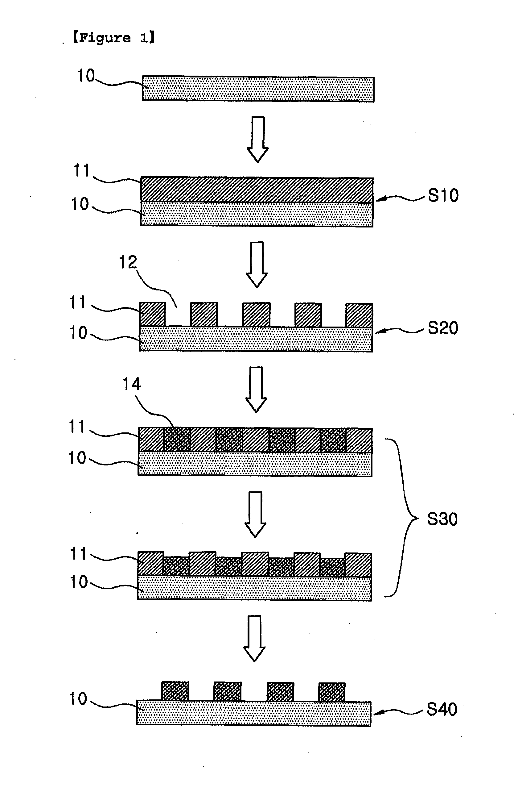
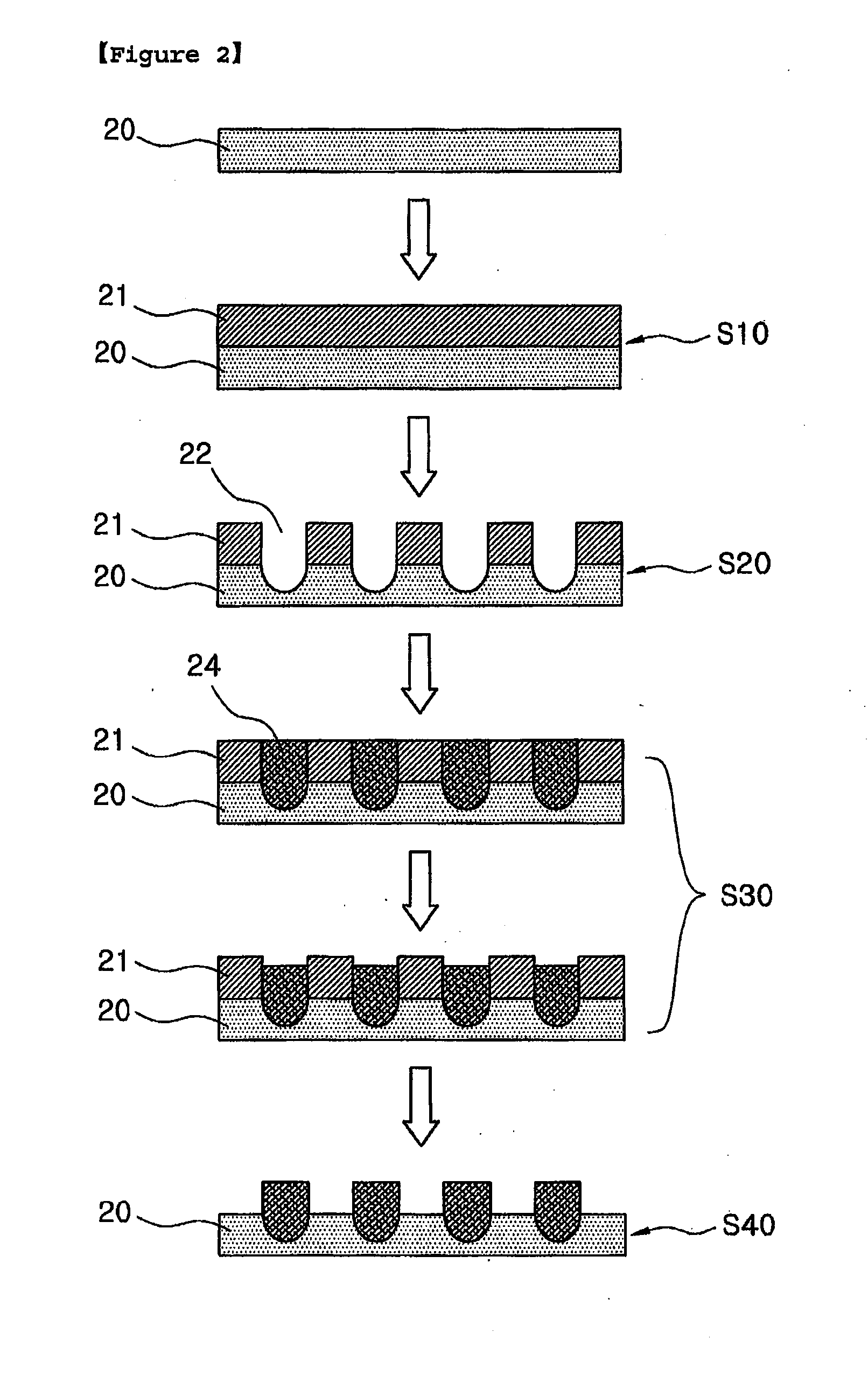
The invention provides a method for making fine blackened conductive patterns. The method is simple and economical, and it doesn't generate any environmental problems. The patterns have high resolution and conductivity. The method involves using a laser beam to pattern the fine patterns, and controlling the laser beam's output energy to control the height of the patterns. The fine patterns can be partially or fully made using an optical diffraction element or mask. The conductive material used in the invention contains silver nanoparticles that have advantages of uniform particle size and minimized cohesion, and can readily form uniform and dense thin film or fine patterns even when the conductive ink has been calcined for a short time at a low temperature. The method can use various conventional methods for forming a layer, such as spin coating, roll coating, spray coating, dip coating, flow coating, doctor blade and dispensing, inkjet printing, offset printing, screen printing, pad printing, gravure printing, flexography printing, stencil printing, or imprinting. After forming a mixture layer containing the conductive material and the blackening material, the fine pattern grooves are filled with the conductive ink, followed by drying and then sequentially filling again with the blackening solution to form the upper blackened layer, thereby completing the formation and blackening of the conductive patterns. The method can also involve removing the resist layer on the substrate to remove any unnecessary portions of the conductive material or the blackening material.

Problems solved by technology

However, the aforementioned conventional photolithography method has problems that the fabrication process is complex and winding, crumpling or tearing may be generated due to an adhesive layer used for the film during transporting process of the fabrication.
Also, high cost and large sized equipments are required according to the etching process and environmental problem may be caused during disposal of the etching solution.
The method of conductive patterns by the screen printing has simple processes, but represents limitation to form high resolution patterns of below 30 um and large area patterns and also has problems of high cost equipment and low productivity.
Although various methods of forming fine patterns using a laser are disclosed as described above, a method of forming blackened fine patterns has not yet been disclosed.

Method used

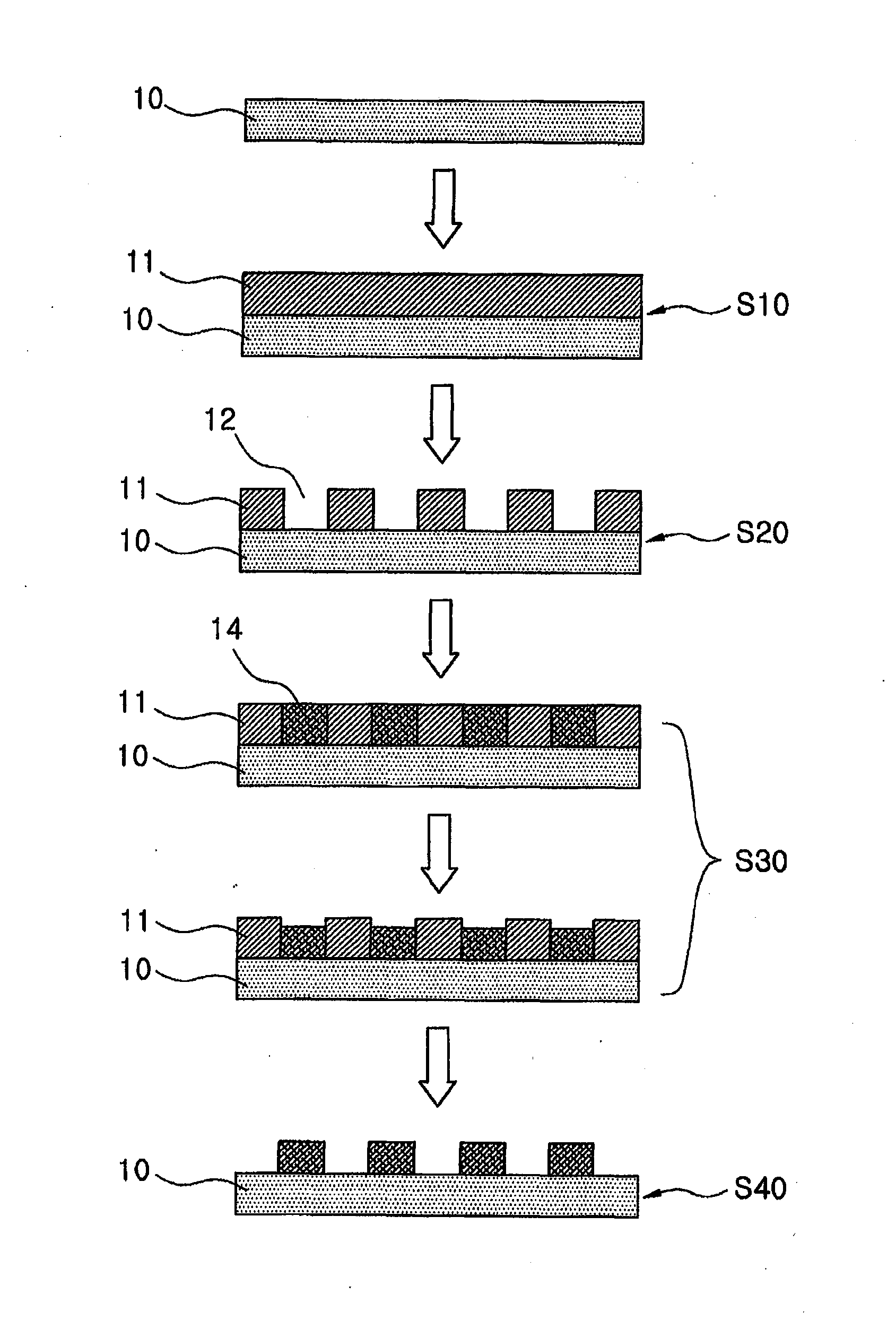

Image

  • Method for Fabricating Blackened Conductive Patterns
  • Method for Fabricating Blackened Conductive Patterns
  • Method for Fabricating Blackened Conductive Patterns

Examples


preparation example 1

Preparation of Silver Complex

[0081]Into a 250 ml Schlenk flask equipped with a stirrer, 34.89 g (129.8 mmol) of viscous liquid in which 2-ethylhexylammonium 2-ethylhexylcarbamate and butylammonium butylcarbamate are mixed at a molar ratio of 7:3 was put and 12.03 g (51.92 mmol) of silver oxide (made by Aldrich Chemical Co.) was added, followed by the reaction at room temperature for two hours with stirring. The reaction solution was initially a black slurry, but it turned transparent as complex was produced. Finally, 46.92 g of yellow, transparent aqueous silver complex was obtained and the silver complex had a viscosity of 7.8 pa·s and a silver content of 23.65 wt % (TGA analysis)

preparation example 2

Preparation of Silver Nanoparticles

[0082]Into a 100 ml beaker, 40.0 g of the silver complex prepared in Preparation Example 1 and 23.1 g of isopropyl alcohol were added and stirred at room temperature for ten minutes to prepare a first solution. Into another 100 ml beaker, 1.2 g of hydrazine monohydrate (made by Daejung Chemicals and Metals Co. Ltd.) and 50 g of isopropyl alcohol were added to prepare a second solution. The first solution and the second solution were injected into their inlets with a flow rate of 20 g / min, respectively. The solutions injected through the inlets were reacted at 5,000 rpm using a stirrer (made by Silverthorne, product name: L4RT-A) to obtain dark green slurry. The prepared slurry was filtered with a 1.2 um filter (made by Wattman company, product name: GF / C) by natural precipitation, followed by washing three times with isopropyl alcohol to obtain green nonopowder.

preparation example 3

Preparation of Conductive Ink

[0083]To 1.2 g of terpineol (made by TCI) as a solvent having a high boiling point, 40.0 g of the silver complex prepared by the same manner as described in Preparation Example 1 and 40 g of the green nanopowder prepared by the same manner as described in Preparation Example 2 were added and stirred for ten minutes, followed by adding 1.2 g of 1-amino-2-propanol (made by Aldrich Chemical Co.) and stirring again for tem minutes. After that, the resultant was passed through a three roll mill (made by Drais Manheim) three times to prepare a conductive ink composition having a silver content of 59.93 wt %.


PUM

PropertyMeasurementUnit
thicknessaaaaaaaaaa
thicknessaaaaaaaaaa
temperatureaaaaaaaaaa

Abstract

The present invention relates to a method for fabricating blackened conductive patterns, which includes (i) forming a resist layer on a non-conductive substrate; (ii) forming fine pattern grooves in the resist layer using a laser beam; (iii) forming a mixture layer containing a conductive material and a blackening material in the fine pattern grooves; and (iv) removing the resist layer remained on the non-conductive substrate.

Description

CROSS REFERENCE TO RELATED APPLICATIONS[0001]This application is a continuation of U.S. patent application Ser. No. 12 / 747,331, filed Sep. 20, 2010, entitled “Method for Fabricating Blackened Conductive Patterns”, which is the United States National Phase of International Patent Application No. PCT / KR2008 / 007307, filed Dec. 10, 2008, which claims the priority of Korean Patent Application No. 10-2007-0128149, filed Dec. 11, 2007, each of which is hereby incorporated by reference herein in its entirety.TECHNICAL FIELD[0002]The present invention relates to a method for fabricating blackened conductive patterns, and more particularly, to a method for fabricating blackened conductive patterns in which a resist layer is formed on a non-conductive substrate using polymer material, fine pattern grooves are formed on the resist layer using a laser beam and then, the blackened conductive patterns are formed in the fine pattern grooves.BACKGROUND ART[0003]Blackening is generally used, for the ...

Claims


Application Information

Patent Timeline
Patent Type & Authority Applications(United States)
IPC IPC(8): H05K3/18
CPCH05K3/184H05K2203/0723H05K2203/072H05K2203/0548H05K1/092H05K1/097H05K3/107H05K3/1258H05K3/245H05K2201/0112H05K2201/0376H05K2201/09036H05K2203/0568H05K2203/1126B82Y40/00H05K3/02C23C18/165C23C18/1868C23C18/204H05K3/0026
Inventor CHUNG, KWANG CHOONYOO, JI HOONKIM, SU-HANKIM, BYUNG HUN
Owner INKTEC CO LTD
Learn More