High voltage semiconductor device

Active Publication Date: 2014-07-10
FUJI ELECTRIC CO LTD
View PDF2 Cites 29 Cited by
  • Summary
  • Abstract
  • Description
  • Claims
  • Application Information

AI Technical Summary

Benefits of technology

The patent proposes a two-input system using high voltage MOSFETs to reduce power consumption and lower the level shifter's power consumption. The system uses pulses to transmit signals and shortens the on period of the MOSFETs. The patent also describes a simplified HVIC and a high voltage IC with a level shift circuit and a high voltage interconnect wire to prevent breakdown of the insulating film. The patent also addresses the potential malfunction caused by voltage variations in the alternating current output terminal and the auxiliary direct current power source. The technical effects of the patent are to reduce power consumption, improve efficiency, and prevent malfunctions in the circuit.

Problems solved by technology

As a result of this, there is fear that short circuit between the arms of the bridge circuit is caused, or the IGBT 17 is unnecessarily turned off.
However, a power loss due to the current increases particularly when the node of the OUT terminal whose potential varies due to the switching is at a high potential.
With this one-input system, the high voltage MOSFET attains an on condition for a long period, an on current continues to flow during the on period of the high voltage MOSFET, and power consumption increases.
Because of this, the signals are not accepted, thus not resulting in a malfunction.
There is also the problem that the input / output transmission delay time of the high side drive circuit increases in a period for which this input signal and the dV / dt surge are superimposed on each other.
Because of this, the potential gradient is difficult to uniformize in the slit region inside the breakdown voltage structure, and the growth of a depletion layer is suppressed, due to which there is the problem that it is easy to locally cause electric field concentration, and it is difficult to raise a breakdown voltage.
There is more than a little increase in the chip area of the high voltage IC due to this, and an increase in the number of manufacturing steps by adding a high resistance polysilicon formation step is also unavoidable.
Because of this, in the two-input method, when the set side and reset side level shift resistances vary, a difference occurs between the potential changes of the drain nodes of the set side and reset side high voltage MOSFETs when the dV / dt surge is input into the level shift circuit, and there is a possibility that an erroneous signal is transmitted to the logic circuit in the subsequent stage.

Method used


Image

  • High voltage semiconductor device
  • High voltage semiconductor device
  • High voltage semiconductor device

Examples


embodiment 1

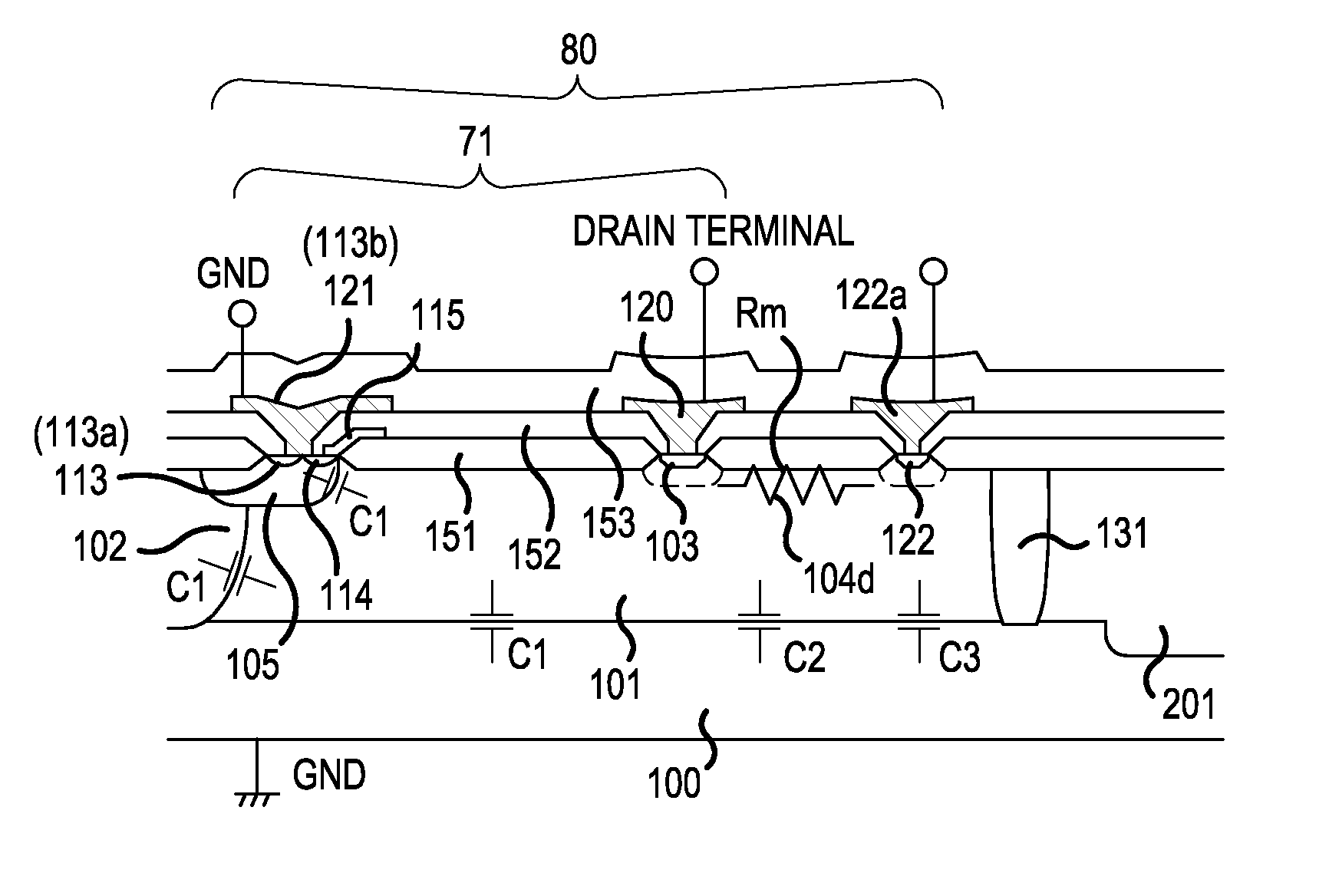
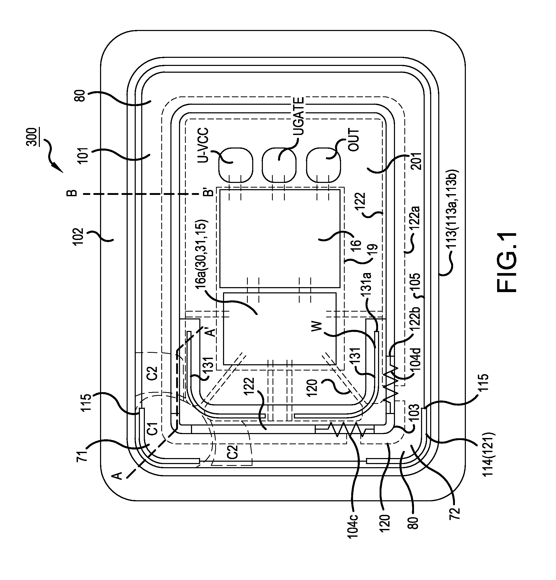
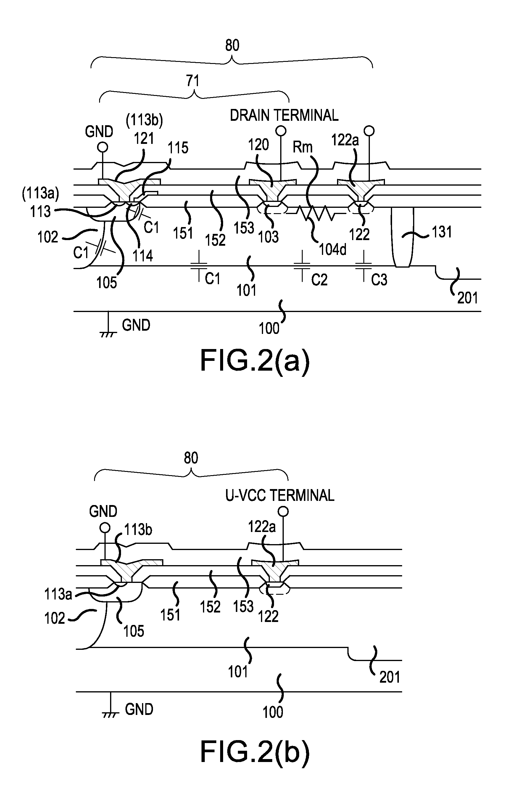
[0109]A description will be given of a structure of a high voltage semiconductor device according to Embodiment 1. FIG. 1 is a plan view showing a main portion of the high voltage semiconductor device 300 according to Embodiment 1 of the invention. The high voltage semiconductor device 300 according to Embodiment 1 of the invention shown in FIG. 1 is a high voltage IC wherein a level shift circuit portion including high voltage MOSFETs 71 and 72 and a drive circuit including a floating potential region are formed on one semiconductor substrate.

[0110]FIGS. 2(a) and 2(b) are sectional views showing a main portion of the high voltage semiconductor device 300 according to Embodiment 1 of the invention. FIG. 2(a) is a main portion sectional view showing a sectional structure along the section line A-A′ of FIG. 1, while FIG. 2(b) is a main portion sectional view showing a sectional structure along the section line B-B′ of FIG. 1.

[0111]The high voltage semiconductor device 300 shown in FIG...

embodiment 2

[0128]Next, a description will be given of a structure of a high voltage semiconductor device according to Embodiment 2. FIG. 3 is a plan view showing a main portion of the high voltage semiconductor device 400 according to Embodiment 2 of the invention. The high voltage semiconductor device 400 is a high voltage IC wherein a level shift circuit portion including high voltage MOSFETs 71 and 72 and a drive circuit including a floating potential region are formed on one semiconductor substrate. The difference of the high voltage semiconductor device 400 according to Embodiment 2 shown in FIG. 3 from the high voltage semiconductor device 300 according to Embodiment 1 shown in FIG. 1 is that the n+drain region 103 and n-type second pick-up region 122 are connected together, and an n buffer region 104 forming a load resistance element is formed in the surface layer of the n−region 101 which is the breakdown voltage region 80. The higher the impurity concentration of a portion of the n−re...

embodiment 3

[0160]Next, a description will be given of a structure of a high voltage semiconductor device according to Embodiment 3. FIG. 7 is a plan view showing a main portion of the high voltage semiconductor device 500 according to Embodiment 3 of the invention. FIGS. 8(a) and 8(b) are sectional views showing a main portion of the high voltage semiconductor device 500 according to Embodiment 3 of the invention. FIG. 8(a) is a main portion sectional view showing a sectional structure along the section line E-E′ of FIG. 7. FIG. 8(b) is a main portion sectional view showing a sectional structure along the section line F-F′ of FIG. 7. The high voltage semiconductor device 500 according to Embodiment 3 is a high voltage IC wherein a level shift circuit portion including high voltage MOSFETs and a drive circuit including a floating potential region are formed on one semiconductor substrate.

[0161]The difference of the high voltage semiconductor device 500 according to Embodiment 3 shown in FIG. 7 ...


PUM


Abstract

An n well region and an n−region surrounding the n well region are provided in the surface layer of a p−silicon substrate. The n−region includes breakdown voltage regions in which high voltage MOSFETs are disposed. The n well region includes a logic circuit region in which a logic circuit is disposed. A p− opening portion is provided between a drain region of each high voltage MOSFET and the logic circuit region. An n buffer region used as load resistances is provided between a second pick-up region and the drain region. The p−opening portion is provided between the n buffer region and logic circuit region. By so doing, it is possible to realize a reduction in the area of chips, and provide a high voltage semiconductor device having a level shift circuit with a high switching response speed.

Description

CROSS-REFERENCE TO RELATED CASES[0001]This application is a continuation of International Application No. PCT / JP2012 / 073426, filed on Sep. 13, 2012, which is based on and claims priority to Japanese Patent Application No. JP 2011-202681, filed on Sep. 16, 2011. The disclosure of the Japanese priority application and the PCT application in their entirety, including the drawings, claims, and the specification thereof, are incorporated herein by reference.BACKGROUND[0002]1. Field of the Invention[0003]The present invention relates to a high voltage semiconductor device having a level shift circuit.[0004]2. Related Art[0005]A power device such as an IGBT (isolated gate bipolar transistor) or a power MOSFET (insulated gate field effect transistor) is utilized in many fields such as in a motor control inverter, as well as in a power source application to a PDP (plasma display panel), a liquid crystal panel, or the like, an inverter for a home electric appliance such as an air conditioner ...

Claims


Application Information

Patent Timeline
IPC IPC(8): H01L29/739H01L29/78
CPCH01L29/7393H01L29/7816H01L27/0629H01L27/088H01L29/0653H01L21/761H01L29/7832
Inventor YAMAJI, MASAHARU
Owner FUJI ELECTRIC CO LTD
Why Eureka
Try Eureka