Field effect transistor which can be biased to achieve a uniform depletion region

a field effect transistor and depletion region technology, applied in the direction of diodes, semiconductor devices, electrical apparatus, etc., can solve the problems of large losses, large losses in this high resistance region, and reduce the efficiency of the jfet, so as to reduce the depletion region, eliminate pinching, and high resistance region

Inactive Publication Date: 2017-12-07
GRAYZEL ALFRED I
View PDF1 Cites 1 Cited by
  • Summary
  • Abstract
  • Description
  • Claims
  • Application Information

AI Technical Summary

Benefits of technology

[0014]The FET of the present invention is superior because there is no pinch-off and hence no high resistance region of length ΔL. This is accomplished by dividing the gate electrode into segments which are insulated from one another and can be biased separately. By biasing each segment separately it is possible to compensate for the voltage distribution along the channel due to the drain voltage thus minimizing the depletion region and eliminating pinch-off. Minimizing the depletion region results in greater efficiency than can be obtained by prior art.

Problems solved by technology

The drain current flows through this depleted region of length ΔL resulting in large losses in this high resistance region.
These losses reduce the efficiency of the JFET.
The drain current flows through this region resulting in large losses.
These losses reduce the efficiency of the MOSFET.
In prior art for all FETs, when a voltage Vdsat is applied from the drain to the source in all FETs the channel will pinch-off causing a loss in efficiency.

Method used


Image

  • Field effect transistor which can be biased to achieve a uniform depletion region
  • Field effect transistor which can be biased to achieve a uniform depletion region
  • Field effect transistor which can be biased to achieve a uniform depletion region

Examples


Embodiment Construction

—APPLIED TO A JFET

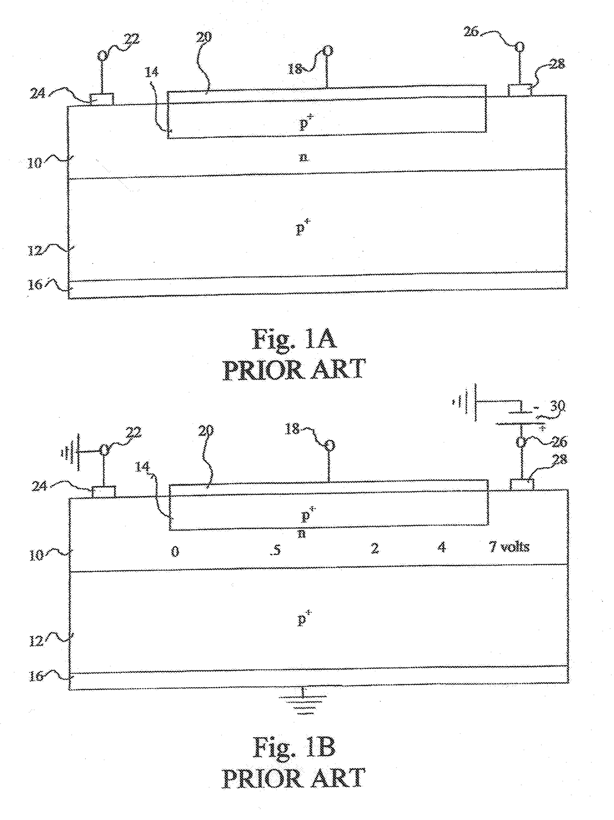
[0030]The invention applies to any Field Effect Transistor (FET). Under normal operation of an FET, a voltage is applied to the gate here-to-for referred to as the gate voltage, which is comprised of an RF signal and a DC bias voltage here-to-for referred to as the bias. Said bias is used to set the average value of the gate voltage. According to the present invention the gate of the FET is divided into segments which are insulated from one another and can be biased separately. The present invention is applicable to any FET such as but not limited to n-type JFET, p-type JFET, MOSFET, NMOSFET, PMOSFET, CMOSFET, MNOSFET, DIGMOSFET, HIGFET, TFET and HEMPT, in the enhancement mode and in the depletion mode and FETs with multiple channels and with multiple gates where one or more of the gates is divided into segments as described above.

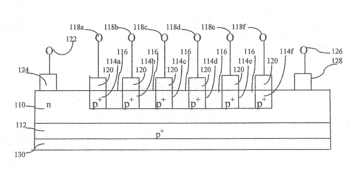
[0031]FIG. 3A shows a JFET according to this invention where N; the number of segments, is equal to six for this example. The active reg...


PUM


Abstract

A Field Effect Transistor including: a channel with one end designated the source and the other end designated the drain; a means for connecting to said source end of said channel; a means for connecting to said drain end of said channel; a gate divided into a plurality of segments each insulated from one another; a means for adjusting the bias of each of said segments independently of one another, whereby the depletion region in said channel can be adjusted to avoid pinch-off and to maximize the efficiency of said Field Effect Transistor.

Description

CROSS REFERENCE TO RELATED APPLICATIONS[0001]This application claims priority to and the benefit of U.S. Provisional Application No. 62 / 392,508, filed Jun. 3, 2016, and entitled “Field Effect Transistor Which has a Uniform Depletion Region Across its Length and Hence Does Not Experience Pichoff,” which application is incorporated by reference herein in its entirety.FIELD OF INVENTION[0002]This invention relates to Field Effect Transistors.BACKGROUND OF THE INVENTION[0003]A Field Effect Transistor by prior art has a channel whose resistance is a function of the gate voltage. All Field Effect transistors have a semiconductor channel with one end labeled the source and the second end labeled the drain. In addition all Field Effect transistors have a gate whose voltage controls the resistance of the channel. Current flowing through the channel is therefore a function of the gate voltage. The gate voltage controls the resistance by creating a depletion region across the channel. In the d...

Claims


Application Information

Patent Timeline
Patent Type & Authority Applications(United States)
IPC IPC(8): H01L29/78H01L27/06H01L29/10H01L29/812H01L29/808
CPCH01L29/7831H01L29/1045H01L29/1058H01L29/8083H01L27/0629H01L29/7827H01L29/8122H01L29/8124H01L29/808H01L29/0649H01L29/1066H01L29/78
Inventor GRAYZEL, ALFRED I.
Owner GRAYZEL ALFRED I
Why Eureka
Try Eureka