
Metal nanoparticle paste, electronic component assembly using metal nanoparticle paste, LED module, and method for forming circuit for printed wiring board

a technology of metal nanoparticles and electronic components, applied in the direction of printed circuit non-printed electrical components association, conductors, conductive pattern formation, etc., can solve the problems of insufficient bonding strength and brittleness of alloys, inability to apply solders to any electrical component or substrate, and inability to meet the requirements of electrical components, etc., to achieve the effect of preventing agglomeration of metal nanoparticles, low cost and mechanical strength

Inactive Publication Date: 2013-10-10
TAMURA KK +1
View PDF3 Cites 18 Cited by
  • Summary
  • Abstract
  • Description
  • Claims
  • Application Information

AI Technical Summary

Benefits of technology

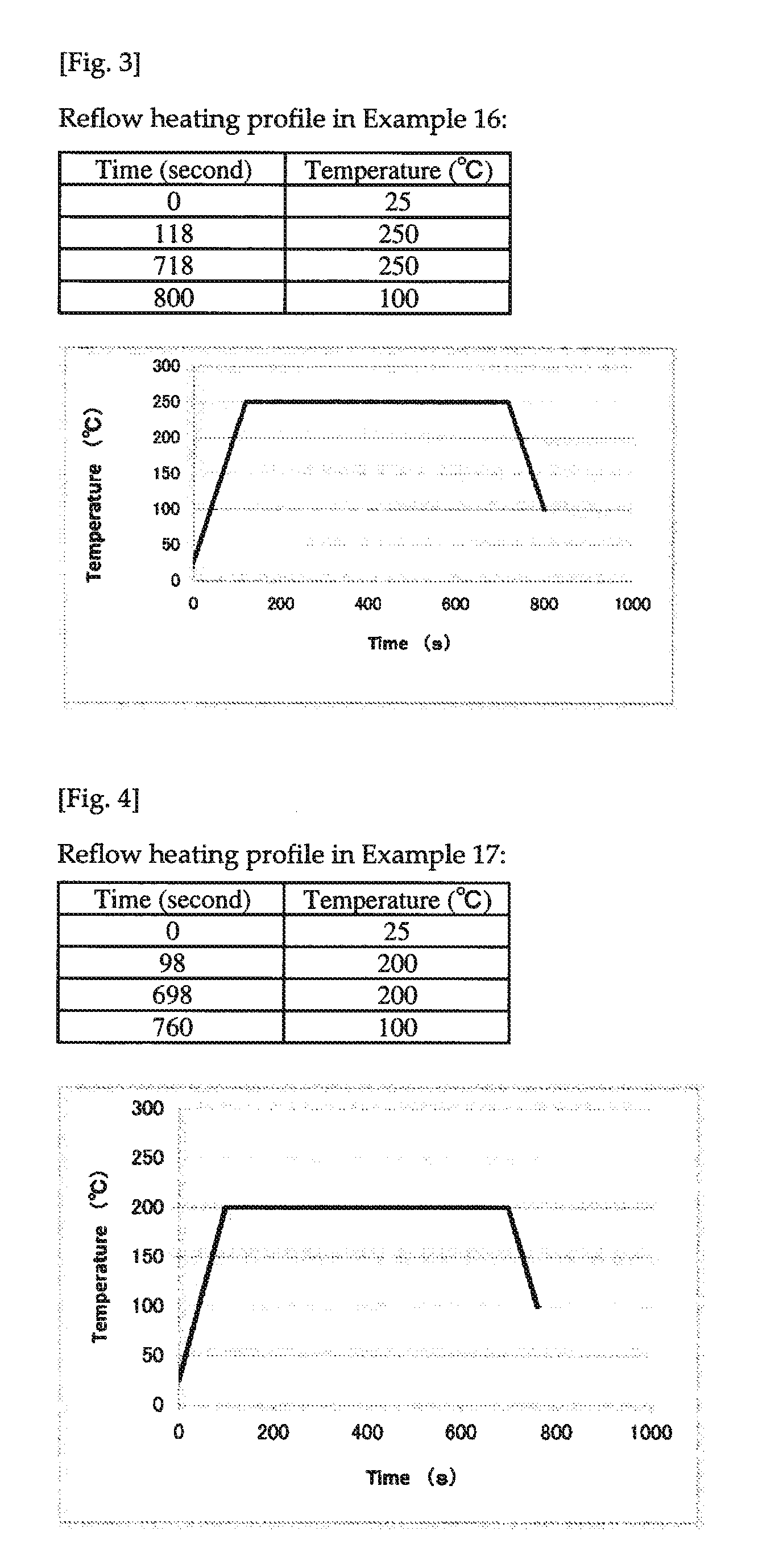
The present invention provides a method to easily and inexpensively achieve metallic bonding and wiring patterns with excellent electrical conductivity and mechanical strength using metal nanoparticles. The surface of the metal nanoparticles is coated with a protective film, which prevents agglomeration and improves dispersion stability during preservation. The metal nanoparticle paste containing silver exhibits excellent electrical conductivity, thermal conductivity, and thermal dissipation properties. Additionally, the paste can be used as a reflectance coating film for circuit boards and for bonding electronic components such as LED elements. The reflow heating profiles show the effectiveness of using metal nanoparticles for soldering and bonding applications.

Problems solved by technology

Since those solders, however, require extremely high mounting temperature such as 240° C. or more, the solders cannot necessarily be applied to any electrical component or substrate.
However, bismuth has disadvantages of insufficient bonding strength and brittleness of alloys thereof, and indium-based alloys have a disadvantage of being expensive.
A silver paste, however, increases electrical resistance by forming a local cell with a tin electrode, causes Kirkendall void formation, and requires high cost.
Recently, heat processes have become more and more complicated, and metal contacts can be exposed to heat several times. In such a case, low melting point alloys such as tin-bismuth alloy involve a problem, i.e., a reduction in bonding reliability due to remelting.
However, a disadvantage such as high cost has not been overcome.

Method used


Image

  • Metal nanoparticle paste, electronic component assembly using metal nanoparticle paste, LED module, and method for forming circuit for printed wiring board
  • Metal nanoparticle paste, electronic component assembly using metal nanoparticle paste, LED module, and method for forming circuit for printed wiring board
  • Metal nanoparticle paste, electronic component assembly using metal nanoparticle paste, LED module, and method for forming circuit for printed wiring board

Examples


examples

[0064]In the following section, the present invention is further described in detail on the basis of examples. The present invention is, however, not limited to the embodiments of the examples described below.

examples 1 to 11

Comparative Examples 1 to 6

[0065]Examples wherein the metal nanoparticle paste according to the present invention is used as an electrically conductive bonding material are described in the following section.

[0066](1) Components of the Metal Nanoparticle Paste:

Electrically Conductive Material:

[0067]Concerning metal nanoparticles coated with protective film (hereinafter referred to as “coated metal nanoparticles”):

Coated Metal Nanoparticles I:

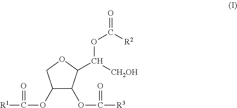
[0068]tin nanoparticles coated with a protective film consisting of the sorbitan fatty acid ester of the formula (I-1), by the above activated continuous-interface vapor-deposition method

Coated Metal Nanoparticles II:

[0069]tin nanoparticles coated with a protective film consisting of the oleyl amine of the formula (IV-1), by the above activated continuous-interface vapor-deposition method

Coated Metal Nanoparticles III:

[0070]silver nanoparticles coated with a protective film consisting of the sorbitan fatty acid ester of the formula (I-1), by the...

examples 12 to 14

Comparative Example 7

[0084]In the following examples, the metal nanoparticle paste in accordance with the present invention was used as a wiring material.

[0085](1) Components of Metal Nanoparticle Paste

Electrically Conductive Material

[0086]Coated metal nanoparticles III and IV were the same as those described in the above examples wherein the metal nanoparticle paste was used as an electrically conductive bonding material. Metal nanoparticles VI were not coated with a protective film.

[0087](2) Process for Producing Metal Nanoparticle Paste Used as Wiring Material:

A predetermined amount of a cyclohexane dispersion containing 20% by weight of coated metal nanoparticles obtained by the above activated continuous-interface vapor-deposition method, was poured into an agate mortar, and the contained cyclohexane was completely volatilized by drying under reduced pressure. Thereby coated metal nanoparticles containing 20% by weight of the protective film component were obtained. Predetermin...


PUM

PropertyMeasurementUnit
mean primary particle diameteraaaaaaaaaa
temperatureaaaaaaaaaa

Abstract

Disclosed is a metal nanoparticle paste that uses the low-temperature sintering characteristics of metal nanoparticles to easily obtain a metal bond with excellent conductivity and mechanical strength, and which can form a wiring pattern with excellent conductivity. The metal nanoparticle paste is characterized by containing (A) metal nanoparticles, (B) a protective film that coats the surface of the metal nanoparticles, (C) a carboxylic acid, and (D) a dispersion medium.

Description

FIELD OF THE INVENTION[0001]The present invention relates to a metal nanoparticle paste comprising metal nanoparticles having a surface coated with a protective film, and a carboxylic acid. More specifically, the present invention relates to a metal nanoparticle paste which makes it possible to form a wiring pattern on a substrate by a heat treatment at an extremely low temperature when printed by screen printing, ink-jet printing or the like, and a metal nanoparticle paste wherewith an electronic component can be bonded onto a substrate by heating at an extremely low temperature.DESCRIPTION OF THE BACKGROUND ART[0002]In the field wherein an electronic component is mounted on a substrate, electrical bonding has been conducted mainly by use of a lead-free solder, particularly a tin-silver-copper alloy solder. Since those solders, however, require extremely high mounting temperature such as 240° C. or more, the solders cannot necessarily be applied to any electrical component or subst...

Claims


Application Information

Patent Timeline
Patent Type & Authority Applications(United States)
IPC IPC(8): C09D11/00H05K1/18H05K1/09
CPCH01B1/22H05K1/097H01L2924/12041H05K3/3484H05K2203/0425H05K2203/122C09D11/52H05K1/181H01L2224/2949H01L24/29H01L24/83H01L2224/293H01L2224/8384H05K3/3431H05K2201/10106H05K2203/1131H01L2924/00H01L2924/15788H01L2924/12042H01L2924/12044H05K3/3485H01B13/00H05K1/09H05K3/10H05K3/12
Inventor NAKATANI, ISAOHIROSE, MASATOHARASHIMA, KEITAKURITA, SATORUKIYOTA, TATSUYA
Owner TAMURA KK
Learn More