Liquid silane-based compositions and methods for producing silicon-based materials
a composition and composition technology, applied in the direction of silicon compounds, conductive materials, pigment addition to spinning solutions, etc., can solve problems such as electrical transport limitation, and achieve the effect of reducing dimensionality and limiting electrical transpor
- Summary
- Abstract
- Description
- Claims
- Application Information
AI Technical Summary
Benefits of technology
Problems solved by technology
Method used
Image
Examples
example 1
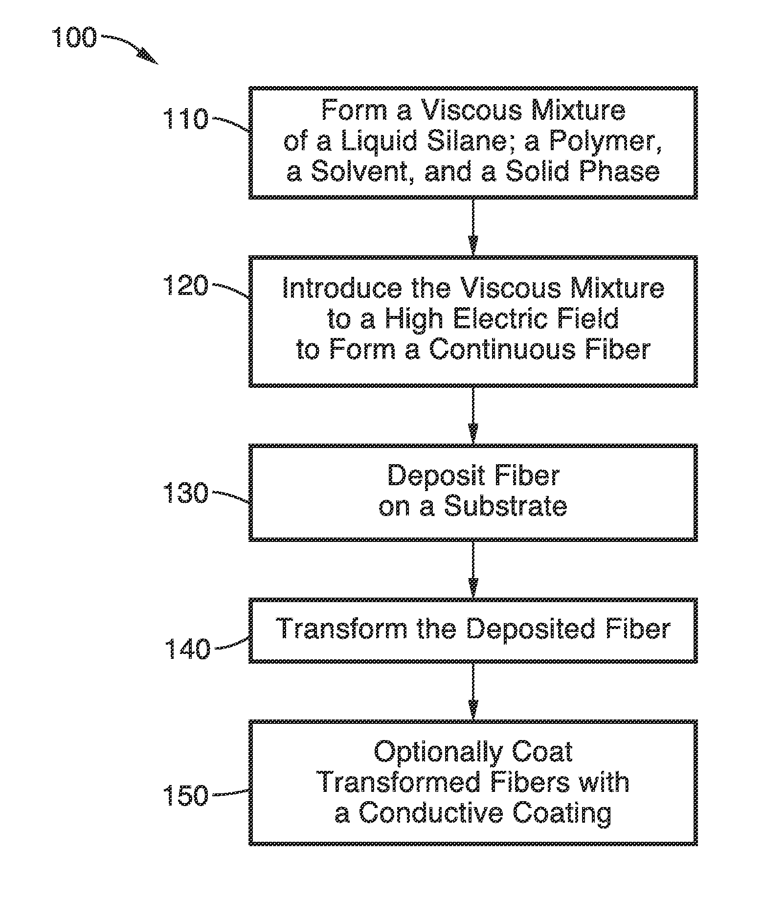
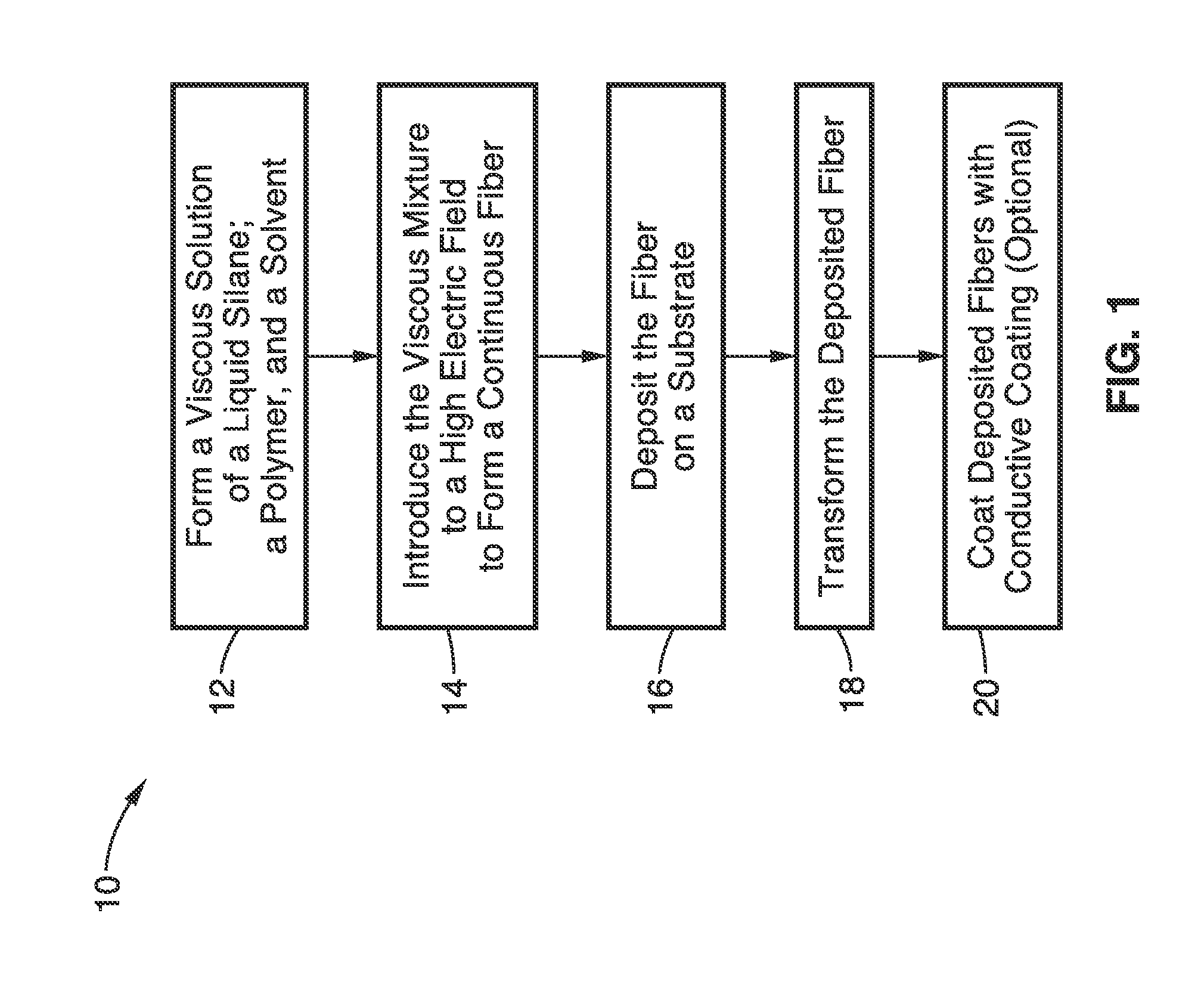
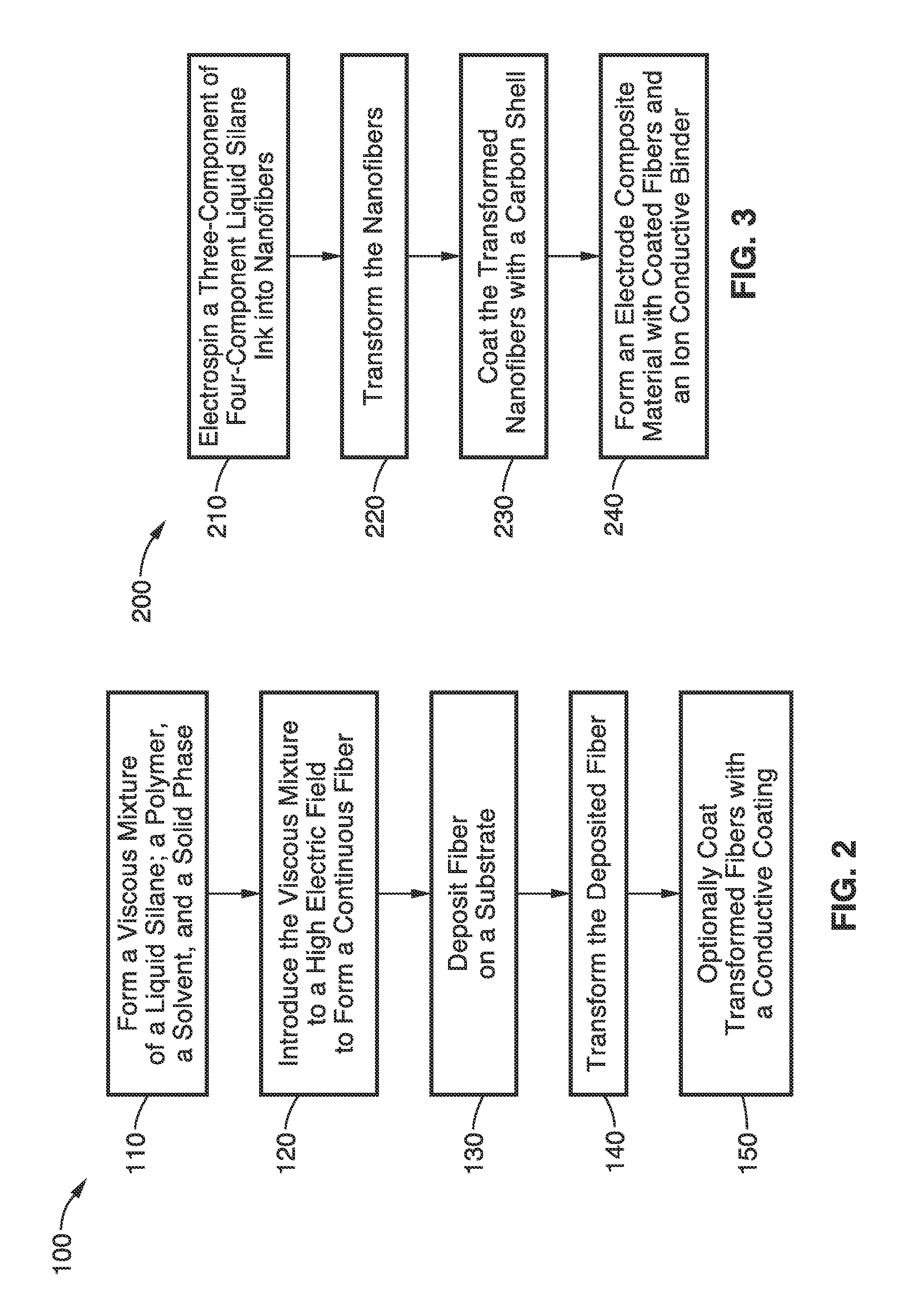
[0083]In order to demonstrate the functionality of the electrospinning methods with different formulations of liquid silane inks, a test reactor was constructed. All electrospinning processing and post-deposition treatments were performed inside inert nitrogen gas gloveboxes with active oxygen scrubbing unless otherwise specified. After appropriate ink formulation, three- and four-component solutions and / or mixtures were taken up into 1 mL HDPE syringes fitted with blunt-nosed 18 gauge stainless steel needles 2.5 cm in length. The ink-containing syringe and needle were placed into a syringe pump in horizontal position with a needle-to-substrate standoff distance of ˜25 cm.
[0084]Metallic copper foil pieces (5 cm×5 cm×0.8 mm) were employed as the electrode substrate in the electrospinning process and were cleaned according to the following protocol: rinsing with ˜5 mL isopropanol using a squirt bottle; rinsing with ˜5 mL 1.5 M hydrochloric acid using a squirt bottle; rinsing with ˜10 ...
example 2
[0091]Electrospinning of a three-component ink, Si6H12 / PMMA using the solvent dichloromethane (DCM), was conducted to demonstrate an alternative solvent and to characterize performance of the resulting material as an electrode. A solution of PMMA in DCM was prepared by adding 18.0 mL of dry DCM to a flame-dried vial with 2.681 g of PMMA mixed via magnetic stirring at 500 RPM for 3 h. Next, 8.220 g of this PMMA / DCM solution, 858 μL of DCM and 418 μL of Si6H12 were added dropwise while magnetically stirring to give a mixture of two immiscible liquids. After stirring for 15 minutes, the mixture appeared to be homogeneous with an apparent viscosity that was higher than either of the immiscible phases indicating the formation of a three-component microemulsion or a single-phase mixture. Electrospinning was realized as described above using a copper foil as the substrate.
[0092]Immediately after electrospinning each 1 mL aliquot, the deposited wires were scraped off of the copper foil and ...
example 3
[0095]The product of a second three-component ink, Si5H10 / PMMA in DCM with a post deposit treatment of 550° C. for 60 minutes and laser exposure was characterized. A 10 wt % polymer solution was prepared by adding dried and nitrogen-sparged DCM into a flame-dried glass vial with PMMA dissolved by stirring for ˜12 h. At that time, 45 μL of Si5H10 was added to the solution using a micropipette and this mixture was stirred for 10 minutes using a PTFE-coated magnetic stir bar. The copper foil substrate was cleaned and moved into the electrospinning glovebox before being mounted and connected to the apparatus. Electrospinning was performed with a 20 cm stand-off distance, a 12 kV excitation, 0.5 mL / h ink flow rate and a total solution volume of ˜75 μL was dispensed.
[0096]Post thermal treatment of the electrospun sample on copper foil was conducted in a nitrogen ambient (2 and H2O). The sample was placed on a room temperature ceramic hotplate, and covered with an aluminum heat shield to i...
PUM
| Property | Measurement | Unit |
|---|---|---|
| Temperature | aaaaa | aaaaa |
| Temperature | aaaaa | aaaaa |
| Temperature | aaaaa | aaaaa |
Abstract
Description
Claims
Application Information
 - R&D
- Intellectual Property
- Life Sciences
- Materials
- Tech Scout
- Unparalleled Data Quality
- Higher Quality Content
- 60% Fewer Hallucinations
Browse by: Latest US Patents, China's latest patents, Technical Efficacy Thesaurus, Application Domain, Technology Topic, Popular Technical Reports.
© 2025 PatSnap. All rights reserved.Legal|Privacy policy|Modern Slavery Act Transparency Statement|Sitemap|About US| Contact US: help@patsnap.com


