Method of Manufacturing a Circuit Carrier Layer and a Use of Said Method for Manufacturing a Circuit Carrier
a manufacturing method and technology of a circuit carrier, applied in the manufacture of multilayer circuits, electrical apparatus, printed circuits, etc., can solve the problems of inability to produce inability to meet the requirements of ultra fine line geometries, etc., to achieve easy and cost-effective production, reduce the loss of high frequency signal integrity, and produce the finest conductor structures.
- Summary
- Abstract
- Description
- Claims
- Application Information
AI Technical Summary
Benefits of technology
Problems solved by technology
Method used
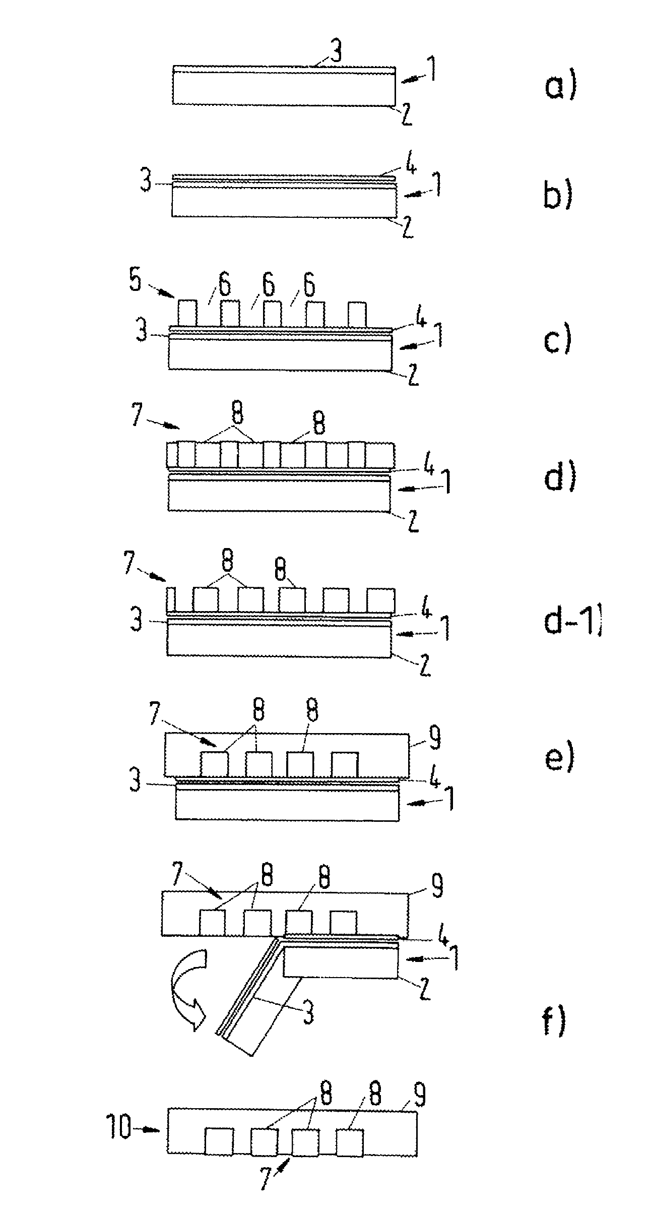
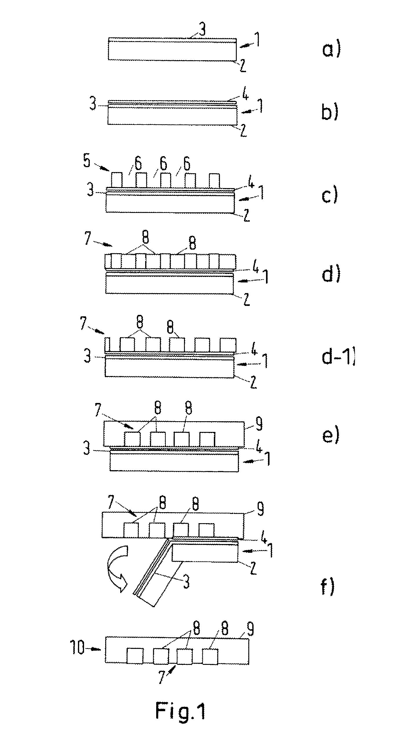
Image

Examples
example 1
Comparative Example
[0079]The auxiliary substrate 1 was immersed for 60 s at 35° C. in a composition consisting of 50 ml / l of 96 wt.-% sulfuric acid, 30 mg / l 5-carboxybenzotriazole and water and dried prior to application of the dry film photoresist. The coating of 5-carboxybenzotriazole served as the release layer 4.
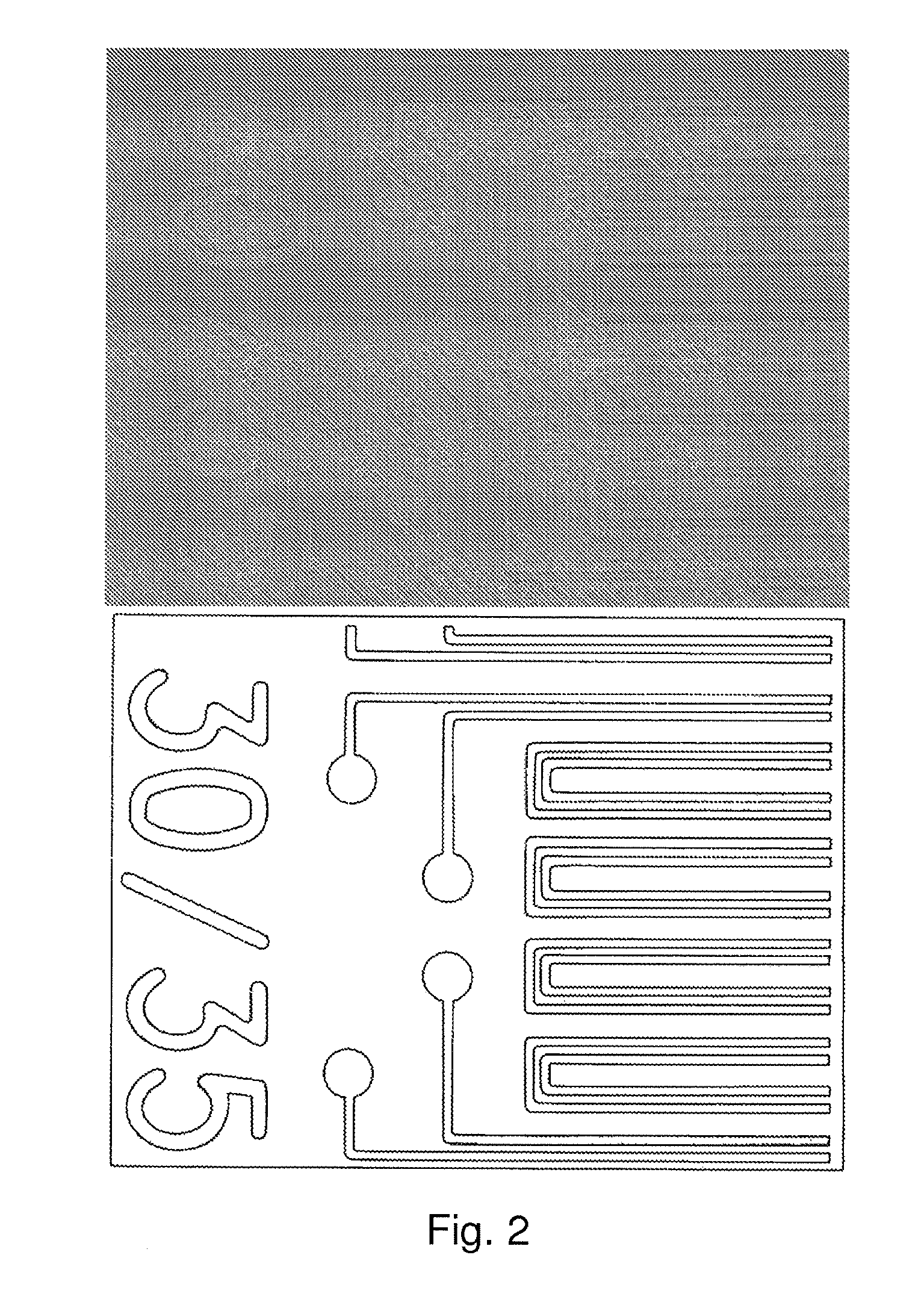
[0080]An optical micrograph of the structured side (side which should have the embedded circuit structure) is shown in FIG. 2. The trenches were not filled with the copper conductor pattern 7, i.e., 5-carboxybenzitriazole did not serve as a release layer 4 forming compound. The copper conductor pattern firmly sticked to the copper layer 3 of the auxiliary substrate 1 when same was peeled off from the dielectric and therefore was transferred to the auxiliary substrate. Consequently, the light structures shown in the photograph of FIG. 2 indicate that no copper was contained in the dielectric.
example 2
Example of the Invention
[0081]The auxiliary substrate 1 was immersed for 60 s at 35° C. in a composition consisting of 30 mg / l 1H-1,2,4-triazole-3-thiol and water prior to application of the dry film photoresist.
[0082]An optical micrograph of the structured side is shown in FIG. 3. The trenches were filled with the copper conductor pattern 7, i.e., an aqueous solution of 1H-1,2,4-triazole-3-thiol served as a release layer 4 forming compound. The dark structures shown in this photograph indicate that copper formed the structures and that the copper did not stick to the copper foil of the auxiliary substrate, but stayed in the dielectric when the auxiliary substrate containing the circuitry was peeled off from the dielectric.
example 3
Example of the Invention
[0083]The auxiliary substrate 1 was immersed for 60 s at 35° C. in a composition consisting of 30 mg / l 1H-1,2,4-triazole-3-thiol, 50 ml / l sulfuric acid (96 wt.-%) and water prior to application of the dry film photoresist.
[0084]The trenches were completely filled with the copper conductor pattern 7 after peeling the circuitry 8 off from the auxiliary substrate 1.
PUM
| Property | Measurement | Unit |
|---|---|---|
| width | aaaaa | aaaaa |
| thick | aaaaa | aaaaa |
| concentration | aaaaa | aaaaa |
Abstract
Description
Claims
Application Information
 - R&D
- Intellectual Property
- Life Sciences
- Materials
- Tech Scout
- Unparalleled Data Quality
- Higher Quality Content
- 60% Fewer Hallucinations
Browse by: Latest US Patents, China's latest patents, Technical Efficacy Thesaurus, Application Domain, Technology Topic, Popular Technical Reports.
© 2025 PatSnap. All rights reserved.Legal|Privacy policy|Modern Slavery Act Transparency Statement|Sitemap|About US| Contact US: help@patsnap.com