Method for manufacturing nitride semiconductor laser element
- Summary
- Abstract
- Description
- Claims
- Application Information
AI Technical Summary
Benefits of technology
Problems solved by technology
Method used
Image

Examples
example 1
Nitride Semiconductor Laser Element
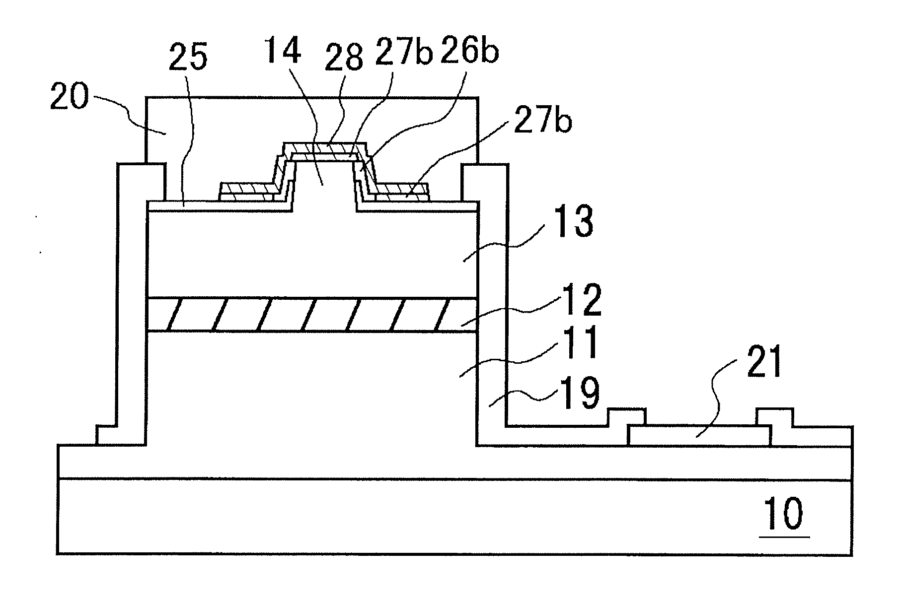
[0138]The laser element in this Example is an element that oscillates in the 500 nm band or lower, and as shown in FIG. 8, an n-side clad layer (2 μm) composed of silicon-doped Al0.33Ga0.67N and an n-side light guide layer (0.15 μm) composed of undoped GaN were formed as the n-side semiconductor layer 11 on the substrate 10 composed of n-type GaN. As the active layer 12, a barrier layer (7 nm) composed of silicon-doped In0.02Ga0.98N and a well layer (10 nm) composed of undoped In0.06Ga0.94N were repeated twice, after which a barrier layer (5 nm) composed of silicon-doped In0.02Ga0.98N was formed. Over this, a p-side cap layer (10 nm) composed of magnesium-doped p-side Al0.30Ga0.70N, a p-side light guide layer (0.15 μm) composed of undoped GaN, a p-side clad layer composed of a superlattice layer with a total thickness of 0.6 μm and consisting of a layer (2.5 nm) composed of undoped Al0.05Ga0.95N and a layer (2.5 μm) composed of magnesium-doped GaN,...
example 2
Method for Manufacturing Nitride Semiconductor Laser Element
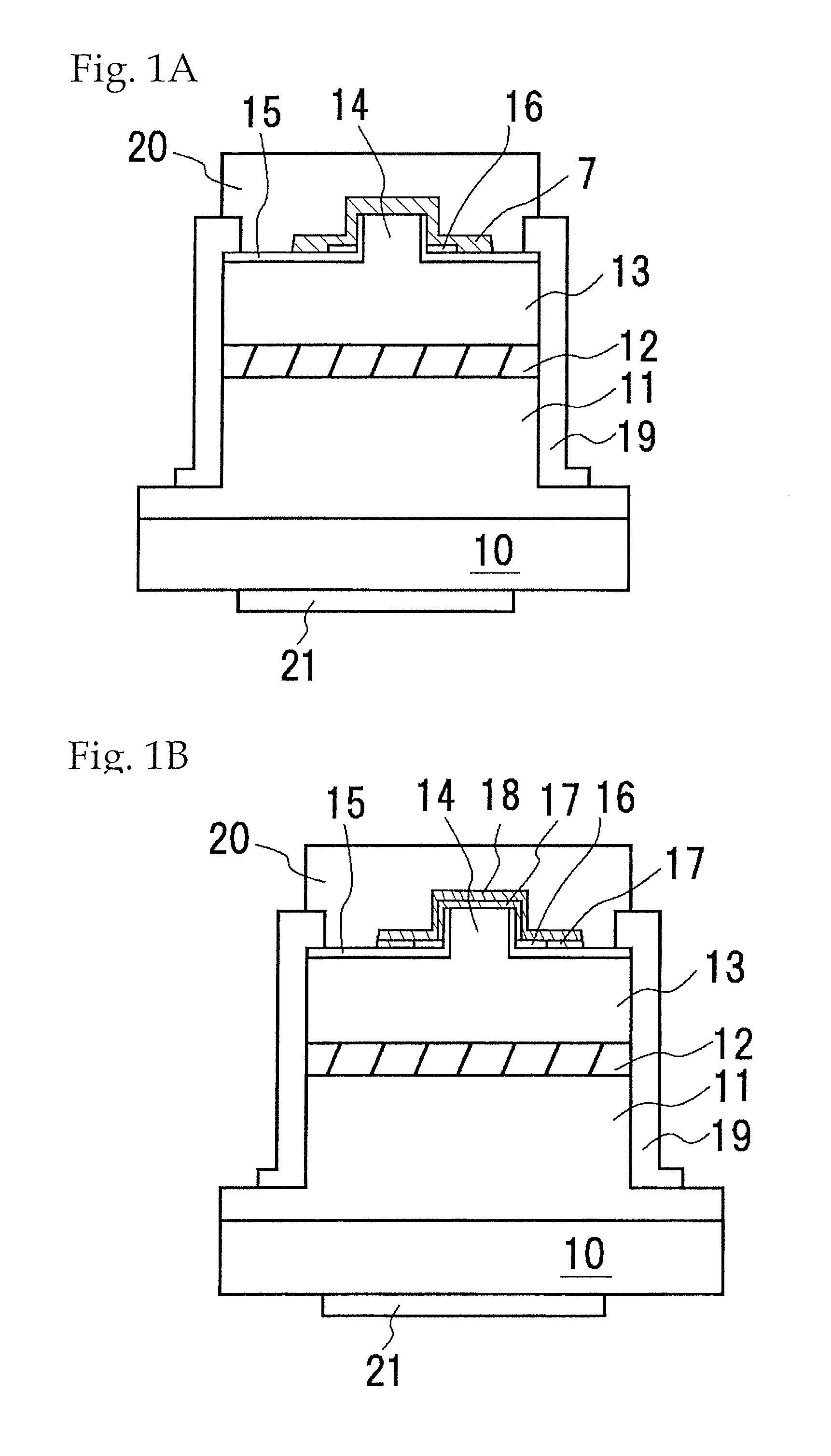
[0148]The laser element of Example 1 can be manufactured by the following method.
(a) Formation of Nitride Semiconductor Layer
[0149]First, a substrate 1 composed of n-type GaN was placed in an MOVPE reaction vessel, and an n-type clad layer composed of silicon-doped Al0.33Ga0.67N was grown using trimethylaluminum (TMA), trimethylgallium (TMG), ammonia (NH3) and silane gas (SiH4; used as an impurity gas). Then, an n-side light guide layer composed of undoped GaN was grown using TMG and ammonia.
[0150]Next, a barrier layer composed of silicon-doped In0.02Ga0.98N was grown using trimethylindium (TMI), TMG, ammonia, and silane gas. The silane gas was halted, and a well layer composed of undoped In0.06Ga0.94N was grown using TMI, TMG, and ammonia. This was repeated twice, after which a barrier layer composed of In0.02Ga0.98N was grown using TMI, TMG, and ammonia, to grow an active layer (refractive index of approximately 2.5) comp...
example 3
Method for Manufacturing Nitride Semiconductor Laser Element
[0168]The laser element of Example 1 can also be manufactured by the following method.
[0169]Everything from the formation of the nitride semiconductor layer in step (a) to the removal of the first protective film in step (d) was carried out in the same manner as in Example 2.
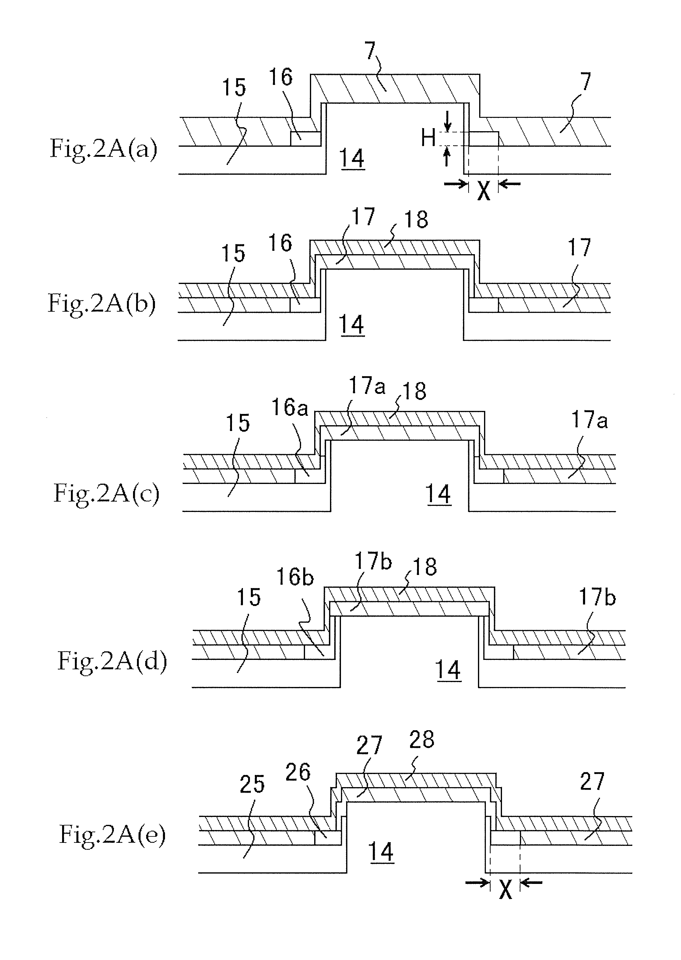
[0170]With the manufacturing method of this Example, the removal of the first protective film in step (d) forms a stepped portion on the side faces of the ridge, and this stepped portion is utilized in step (e) to laminate the conductive layer and form an electrode. With the electrode formed here, gaps are introduced in a portion of the conductive layer 43, which is attributable to the stepped portion of the side faces of the ridge.
(e) Lamination of Conductive Layer
[0171]As shown in FIG. 6 (a), a mask pattern 52 having an opening in the region where the p-side electrode was formed was formed on the nitride semiconductor layer on which the first protecti...
PUM
 Abstract
Description
Claims
Application Information
 - R&D
- Intellectual Property
- Life Sciences
- Materials
- Tech Scout
- Unparalleled Data Quality
- Higher Quality Content
- 60% Fewer Hallucinations
Browse by: Latest US Patents, China's latest patents, Technical Efficacy Thesaurus, Application Domain, Technology Topic, Popular Technical Reports.
© 2025 PatSnap. All rights reserved.Legal|Privacy policy|Modern Slavery Act Transparency Statement|Sitemap|About US| Contact US: help@patsnap.com