
Cleaning solution, cleaning method and damascene process using the same

Active Publication Date: 2012-01-12
UNITED MICROELECTRONICS CORP
View PDF0 Cites 8 Cited by
  • Summary
  • Abstract
  • Description
  • Claims
  • Application Information

AI Technical Summary

Benefits of technology

[0007]The present invention provides a cleaning solution to effectively remove the residues containing a plurality of species.
[0008]The present further invention provides a damascene process to reduce the surface damage (copper loss) of the conductive layer, avoid damages of the dielectric layer or an increase in the dielectric constant, or prevent bridges between the dual damascene structures, and thus, the reliability of the semiconductor device is enhanced.
[0009]The present invention also provides a cleaning method to effectively remove the residues containing a plurality of species.
[0029]According to an embodiment of the present invention, the cleaning solution can effectively remove the residues containing a plurality of species.
[0030]According to an embodiment of the present invention, the damascene process can reduce the surface damage (copper loss) of the conductive layer, avoid damages of the dielectric layer or an increase in the dielectric constant, or prevent bridges between the dual damascene structures, and thus, the reliability of the semiconductor device is enhanced.
[0031]According to an embodiment of the present invention, the cleaning solution can effectively remove the residues containing a plurality of species.

Problems solved by technology

These fluorine-containing gases may react with the TiN hard mask layer to produce titanium fluoride (TiFx) on the surface of the device, and thus, a profile change of the device, abnormal conduction, leakage or short circuiting between film layers is caused, and the reliability of the device is accordingly reduced.
Further, upon the study, the post-etch cleaning process may effect the conduction ability of the device by etching the exposed metal lines below the dual damascene opening, cause a profile change by swelling the dielectric layer with the cleaning solution, or lead to an increase in the dielectric constant.

Method used


Image

  • Cleaning solution, cleaning method and damascene process using the same
  • Cleaning solution, cleaning method and damascene process using the same
  • Cleaning solution, cleaning method and damascene process using the same

Examples


example

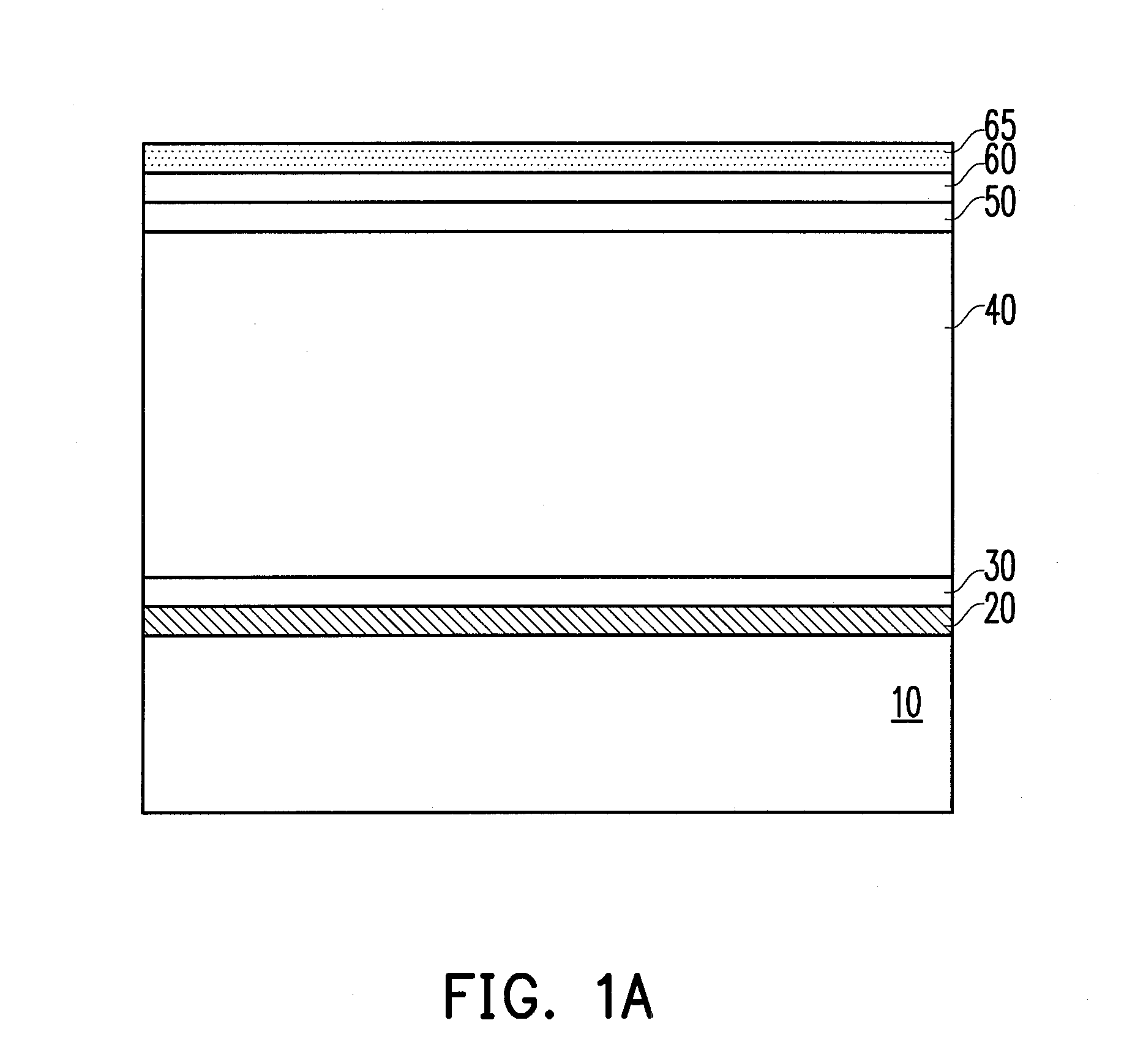
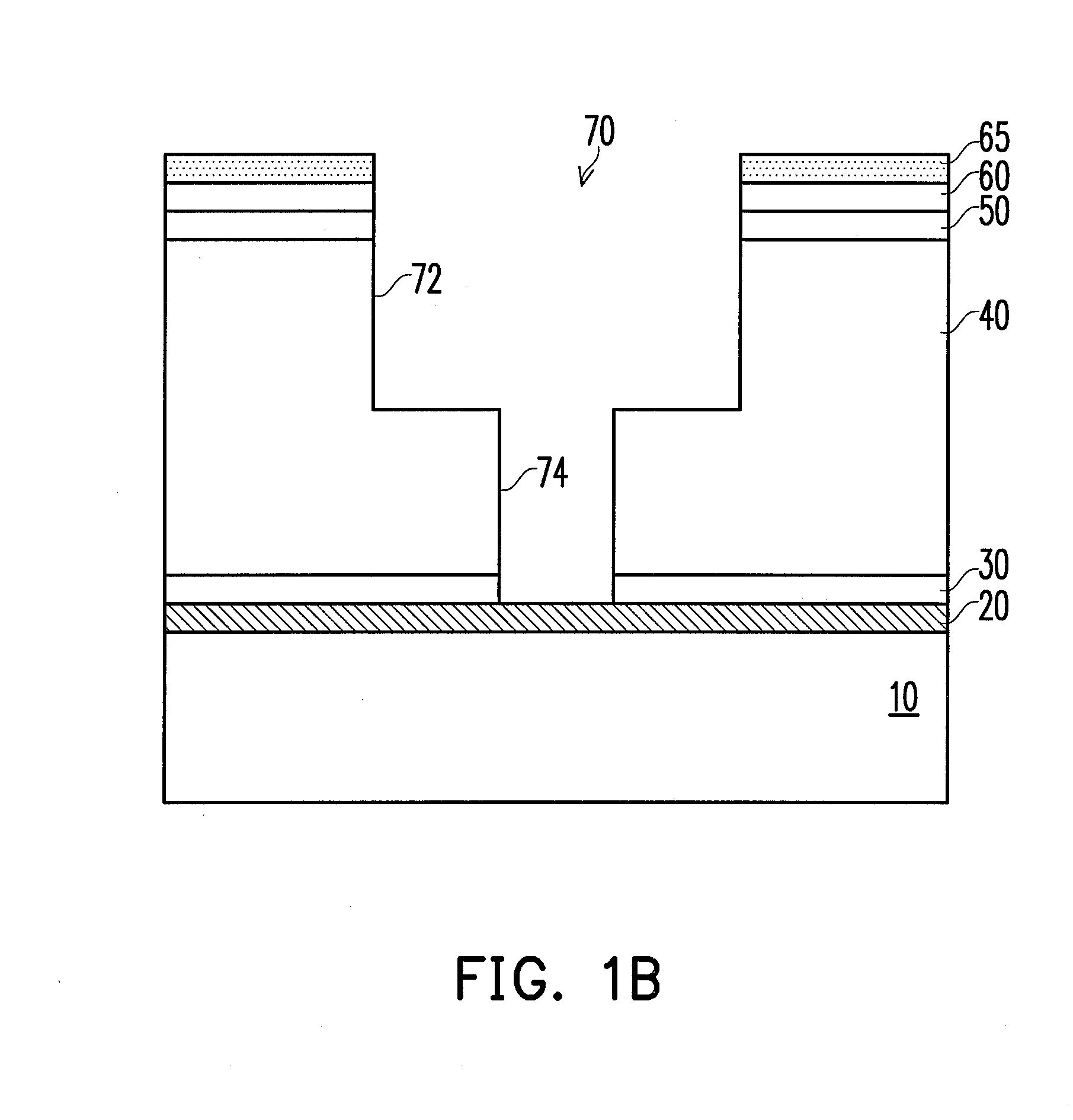
[0048]An ultra low-k dielectric layer, a silicon oxynitride layer and a titanium nitride layer are sequentially formed on a substrate having a copper layer and a carbide silicon nitride layer thereon. Thereafter, a photolithography process is performed and followed by a dry etching process with fluorine containing gases, so as to form a dual damascene opening. Afterwards, a chemical cleaning process is performed with a cleaning solution (0.06 wt % of hydrofluoric acid, 3 wt % of sulfuric acid, 0.1 wt % of ammonia fluoride, 10 wt % of oxalic acid, 10 wt % of TEA, 0.2 wt % of EDTA and water for balance), and then another cleaning process is performed immediately with DI water.

[0049]The result shows that the residues in the process can be effectively removed by performing the chemical cleaning process with the cleaning solution and followed by another cleaning process with DI water. Moreover, damages are not found on the surface of the dielectric layer or the copper layer, or an increa...


PUM


Abstract

A cleaning solution is provided. The cleaning solution includes (a) 0.01-0.1 wt % of hydrofluoric acid (HF); (b) 1-5 wt % of a strong acid, wherein the strong acid is an inorganic acid; (c) 0.05-0.5 wt % of ammonium fluoride (NH4F); (d) a chelating agent containing a carboxylic group; (e) triethanolamine (TEA); (f) ethylenediaminetetraacetic acid (EDTA); and (g) water for balance.

Description

BACKGROUND OF THE INVENTION[0001]1. Field of Invention[0002]The present invention relates to a cleaning solution, a cleaning method and a damascene process using the same.[0003]2. Description of Related Art[0004]A Dual damascene process is a technology widely applied in a semiconductor process. To reduce the RC delay caused by a parasitic capacitance, the current dual damascene process adopts an ultra low-k (ULK) material as a dielectric layer. Further, with the minimization of the device, a titanium nitride (TiN) hard mask layer is formed on the dielectric layer, and then the required patterns are precisely transferred to the dielectric layer by utilizing different etching selectivities of the TiN hard mask layer and the dielectric layer.[0005]The pattern transfer is usually achieved by a dry etching process. However, during the etching process, the reactive gases passing into a reaction chamber may also undergo a polymerization reaction. Therefore, the organic polymer formed from ...

Claims


Application Information

Patent Timeline
IPC IPC(8): H01L21/768C11D3/02B08B3/08
CPCC11D7/08C11D7/265C11D7/3209C11D7/3218H01L21/76814C11D11/0047H01L21/02063H01L21/31144C11D7/3245C11D2111/22
Inventor LIU, AN-CHILAN, TIEN-CHENG
Owner UNITED MICROELECTRONICS CORP
Learn More