Methods of Coating Substrate With Plasma Resistant Coatings and Related Coated Substrates
a technology of coating substrate and coating material, which is applied in the direction of electric/magnetic/electromagnetic heating, instruments, transportation and packaging, etc., can solve the problems of limiting application, coating materials may react with plasma components, and generating unwanted particulates, etc., and achieves the effect of reducing particulation
- Summary
- Abstract
- Description
- Claims
- Application Information
AI Technical Summary
Benefits of technology
Problems solved by technology
Method used
Image
Examples
example i
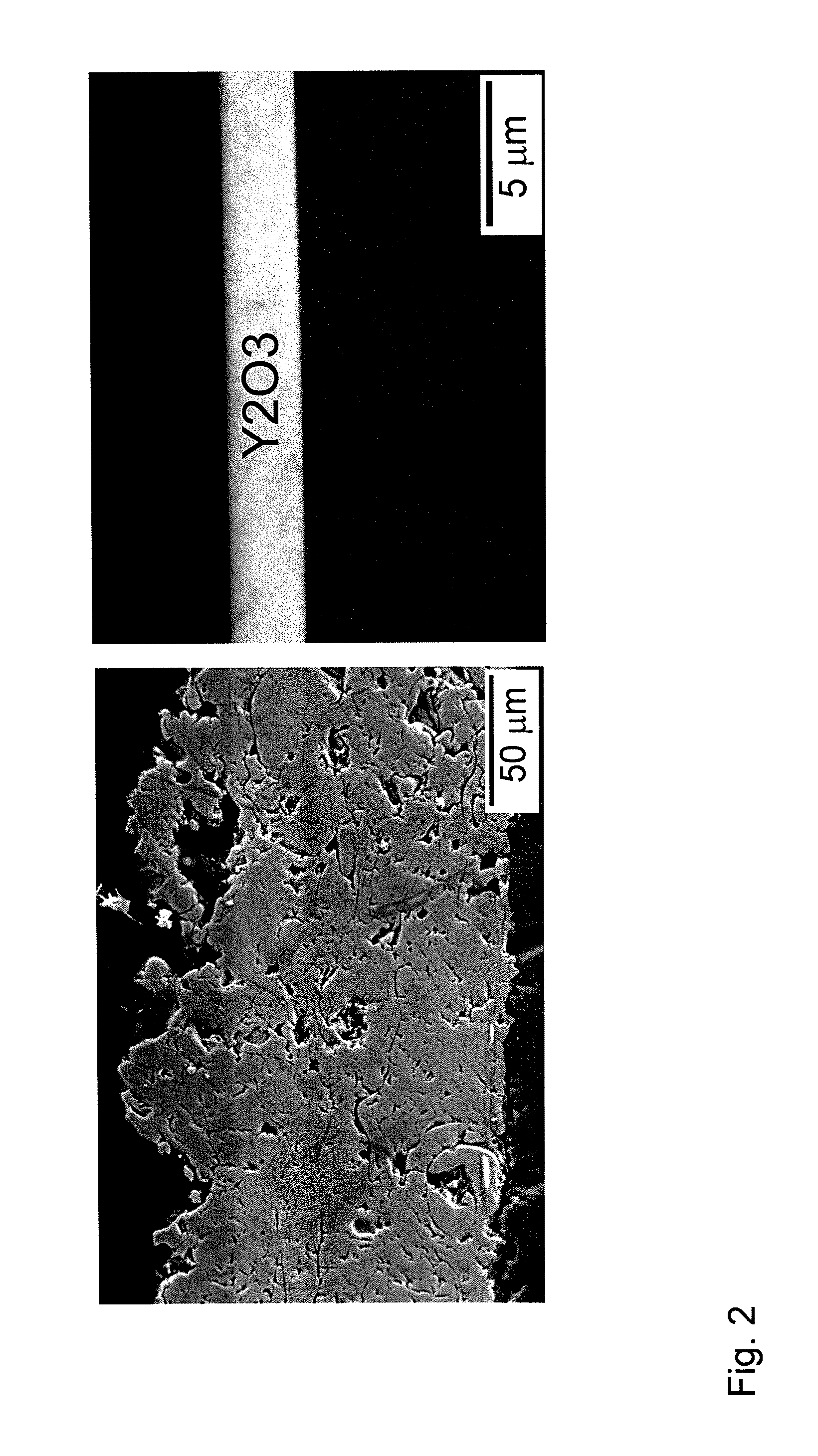
[0048]Quartz disc made of fused quartz (500 mm diameter×50 mm thick) to be used for 300 mm wafer plasma etching chamber was prepared used as a coating substrate. The disc was ultrasonically cleaned with isopropyl alcohol. Then the disc was installed in electron beam coating chamber and remained under vacuum overnight. The coating chamber vacuum level was kept at 2.4×10⁻⁵ torr and preheated to 200° C. for 1 h. High purity yttria target (>99.99%) was evaporated by electron beam and coated for 5 h to obtain a 5 micron coating thickness. Argon ion beam was used to assist electron beam coating. After the coating, the sample was etching tested in SF6 for 10 h. No particulation or etching was observed. The etching rate was measured from the difference in coating thickness between plasma exposed area and masked area. The specimen was partially masked with monolithic yttria ceramics. After the plasma etching experiment, the difference in height was measured with surface profilometer. The mea...
example ii
[0049]A silicon focus ring (360 mm diameter×3.4 mm thick) was used to make an yttria coating. The substrate was ultrasonically cleaned with isopropyl alcohol. Then the ring was cut into small pieces and partially coated in the same way mentioned in Example 1. The coating thickness was 7 micron at the top surface and 3-5 micron at the edge. The focus ring was exposed direct NF3 plasma (35 sccm NF3, 3 sccm O2, 500 mTorr and 350 watt) for 2 h.
[0050]FIG. 9 shows the typical example of partially coated silicon focus ring. As coated specimen shows the difference in contrast. The coated region 90 is slightly darker than uncoated region 91. The boundary was shown with a curved line. After 2 h etching, the coated region 95 is not etched at all, but the uncoated region 96 is etched 1.5 mm deep. The silicon focus ring was attacked from uncoated side as well. Yttria film 97 is still observed to remain on the surface of silicon ring. The underneath portion was etched away.
example iii
[0051]An aluminum coupon (30×30×3 mm), were used to make an yttria coating. The substrate was coated in the same way mentioned in Example 1. The coating thickness was 5 micron. The coated sample was plasma etch tested in direct NF3 plasma. The etching condition was 35 sccm of NF3, 3 sccm of O2, 500 mTorr and 350 watt plasma power. The sample was etched for 8 h. No damage on the coating surface was observed after plasma etching. The etched sample was cross cut and the coating thickness measured by SEM was compared with the sample before plasma etching. The etching rate was less than 3 nm / h in case of the coating on aluminum metal.
PUM
| Property | Measurement | Unit |
|---|---|---|
| thickness | aaaaa | aaaaa |
| time | aaaaa | aaaaa |
| time | aaaaa | aaaaa |
Abstract
Description
Claims
Application Information
 - R&D
- Intellectual Property
- Life Sciences
- Materials
- Tech Scout
- Unparalleled Data Quality
- Higher Quality Content
- 60% Fewer Hallucinations
Browse by: Latest US Patents, China's latest patents, Technical Efficacy Thesaurus, Application Domain, Technology Topic, Popular Technical Reports.
© 2025 PatSnap. All rights reserved.Legal|Privacy policy|Modern Slavery Act Transparency Statement|Sitemap|About US| Contact US: help@patsnap.com


