
Nanomechanical photonic devices

a photonic device and nano-mechanical technology, applied in the direction of instruments, material analysis through optical means, optical elements, etc., can solve the problems of significant challenge in on-chip detection of force, large force is generally considered too small for macroscopic practical use, etc., and achieve the effect of adding optical losses or mechanical problems

Active Publication Date: 2011-05-05
YALE UNIV
View PDF12 Cites 12 Cited by
  • Summary
  • Abstract
  • Description
  • Claims
  • Application Information

AI Technical Summary

Benefits of technology

[0012]Cantilevering the waveguide means that a greater range of displacement and hence a greater tuning or attenuation range can be achieved.
[0017]Having one cantilever arm longer than the other means that one can remain relatively stationary and the other can benefit from an increased range of movement thus resulting in further improved tuning or attenuation ranges.
[0019]In this way, the couplers which are normally employed only to couple light into a waveguide may serve a dual purpose thus doing away with the need for additional components which might introduce additional optical losses or mechanical problems.

Problems solved by technology

This force is generally considered too small for macroscopic practical use.
However, the large footprints involved in these optical microcavities fundamentally limit the scaling of devices down to nanoscale dimensions where exciting quantum phenomena such as macroscopic quantum coherence, generation of squeezed states and optical entanglement start to manifest.
Recent theories predicted that the optical force can be enhanced in a photonic waveguide without the aid of a cavity and can be directly used for electromechanical actuation; however, on-chip detection of the force has been a significant challenge, primarily owing to the lack of efficient nanoscale mechanical transducers in the photonics domain.

Method used


Image

  • Nanomechanical photonic devices
  • Nanomechanical photonic devices
  • Nanomechanical photonic devices

Examples


Embodiment Construction

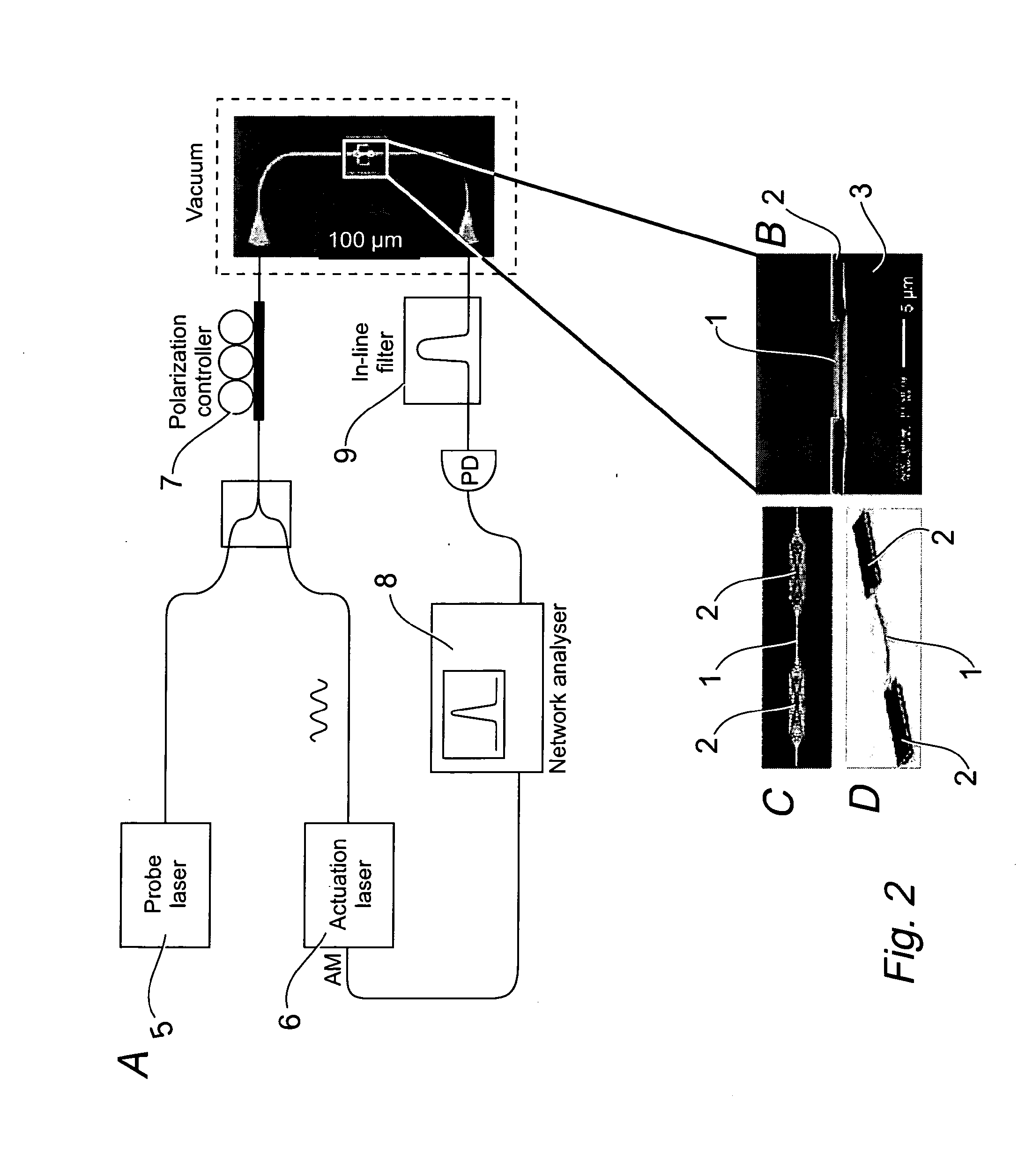
e embodying one or more aspects of the invention which takes the form of a photonic transistor 20.

[0039]FIG. 9a shows in schematic form a photonic switch 30 embodying the invention, and 9b shows a practical application of the photonic switch being employed to cut off an optical sub-circuit which is known to be bad.

[0040]FIG. 10 illustrates end-to-end cantilevered waveguide nanolevers 41,42 embodying one or more aspects of the invention.

[0041]FIG. 11 illustrates a light force tuneable photonic coupler 50 embodying one or more aspects of the invention.

[0042]FIG. 12 illustrates a tuneable phase shifter 60 which operates by optical force which embodies one or more aspects of the invention.

[0043]FIG. 13 illustrates in schematic form a tuneable filter 70 which embodies a number of aspects of the invention, namely a cantilevered waveguide 71, a tuneable coupler 72 and a tuneable phase shifter 73.

[0044]FIG. 14 illustrates a photonic bus synchronised oscillator 80 that embodies one or more a...


PUM


Abstract

The present invention relates to devices which operate on gradient optical forces, in particular, nanoscale mechanical devices which are actuable by gradient optical forces. Such a device comprises a waveguide and a dielectric body, with at least a portion of the waveguide separated from the dielectric body at a distance which permits evanescent coupling of an optical mode within the waveguide to the dielectric body. This results in an optical force which acts on the waveguide and which can be exploited in a variety of devices on a nano scale, including all-optical switches, photonic transistors, tuneable couplers, optical attenuators and tuneable phase shifters. The waveguide can also comprise a gap such that two cantilever bridges are formed.

Description

[0001]This application claims priority from U.S. Provisional Application Nos. 61 / 043,607 and 61 / 117,792, the contents of which are hereby incorporated by reference in their entirety.FIELD OF THE INVENTION[0002]The present invention relates to devices which operate on gradient optical forces, and to methods of manufacturing such devices; in particular, nanoscale mechanical devices which are actuable by gradient optical forces.BACKGROUND OF THE INVENTION[0003]The optical force is one of the most fundamental properties carried by light. This force is generally considered too small for macroscopic practical use. Yet in the microscopic world, optical tweezers have been widely used to manipulate atoms and micron-sized dielectric particles in free space.[0004]One natural step forward would be exploiting this principle as a driving force in solid state devices such as electromechanical systems. Indeed, recent experiments have elucidated the radiation force of light in high finesse optical m...

Claims


Application Information

Patent Timeline
IPC IPC(8): G02F1/01G02B6/35G02B6/26G01N21/84
CPCB82Y20/00G02B6/12007G02B6/122G02B6/283G02B6/3504G02B6/3548G02B6/26G02B6/356G02B6/3568G02B6/3594G02B6/3596G02B2006/12038G02B2006/12061G02B6/3552
Inventor TANG, HONGXINGLI, MOPERNICE, WOLFRAMXIONG, CHI
Owner YALE UNIV
Learn More