
Microelectronic thermal interface

a thermal interface and microelectronic technology, applied in the direction of soldering apparatus, manufacturing tools, light and heating equipment, etc., can solve the problems of reducing heat transfer efficiency, affecting the efficiency of heat dissipation, so as to achieve significant cost and performance advantages, low cost, and high thermal conductivity

Inactive Publication Date: 2011-04-28
KESTER
View PDF4 Cites 44 Cited by
  • Summary
  • Abstract
  • Description
  • Claims
  • Application Information

AI Technical Summary

Benefits of technology

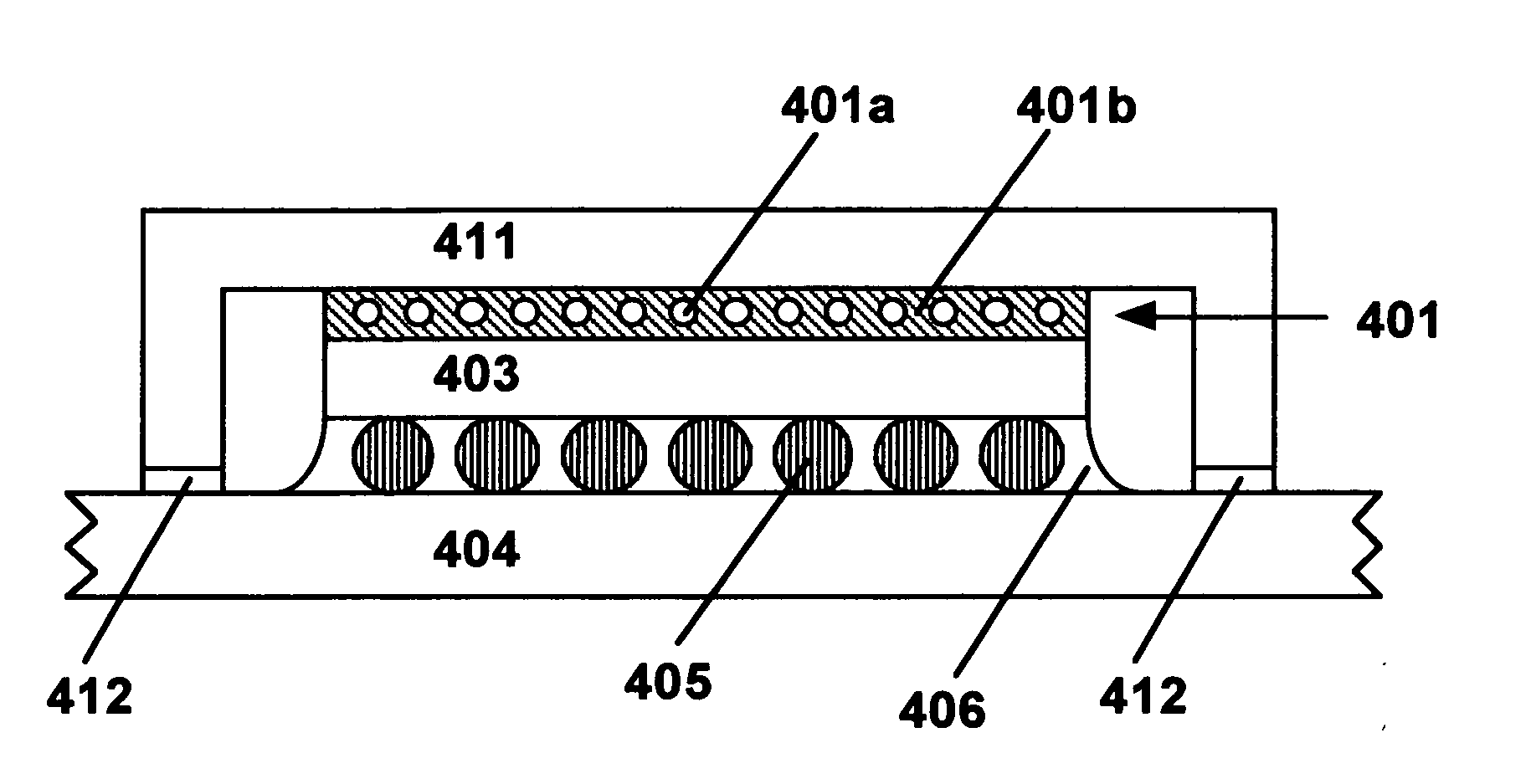
The present invention provides an improved thermal interface between an integrated circuit (IC) chip and a heat sink by using a solder material with a metallic grid embedded in it. The metallic grid helps to enhance heat transfer and reduce hot spots on the IC chip, leading to improved performance and reduced costs. The preform for the thermal interface can be easily fabricated by embedding the metallic grid in a sheet of solder material and heating it. The invention also allows for a reduction in the amount of solder material needed and mitigates solder bleed out and squeeze out, which increases circuit density and reduces costs. The metallic grid also helps to reduce voids in the solder material, improving performance.

Problems solved by technology

As IC chips have decreased in size and increased in speed, heat dissipation has become a significant issue for the microelectronics industry.
In addition, the price of indium has recently increased sharply and fluctuates greatly.
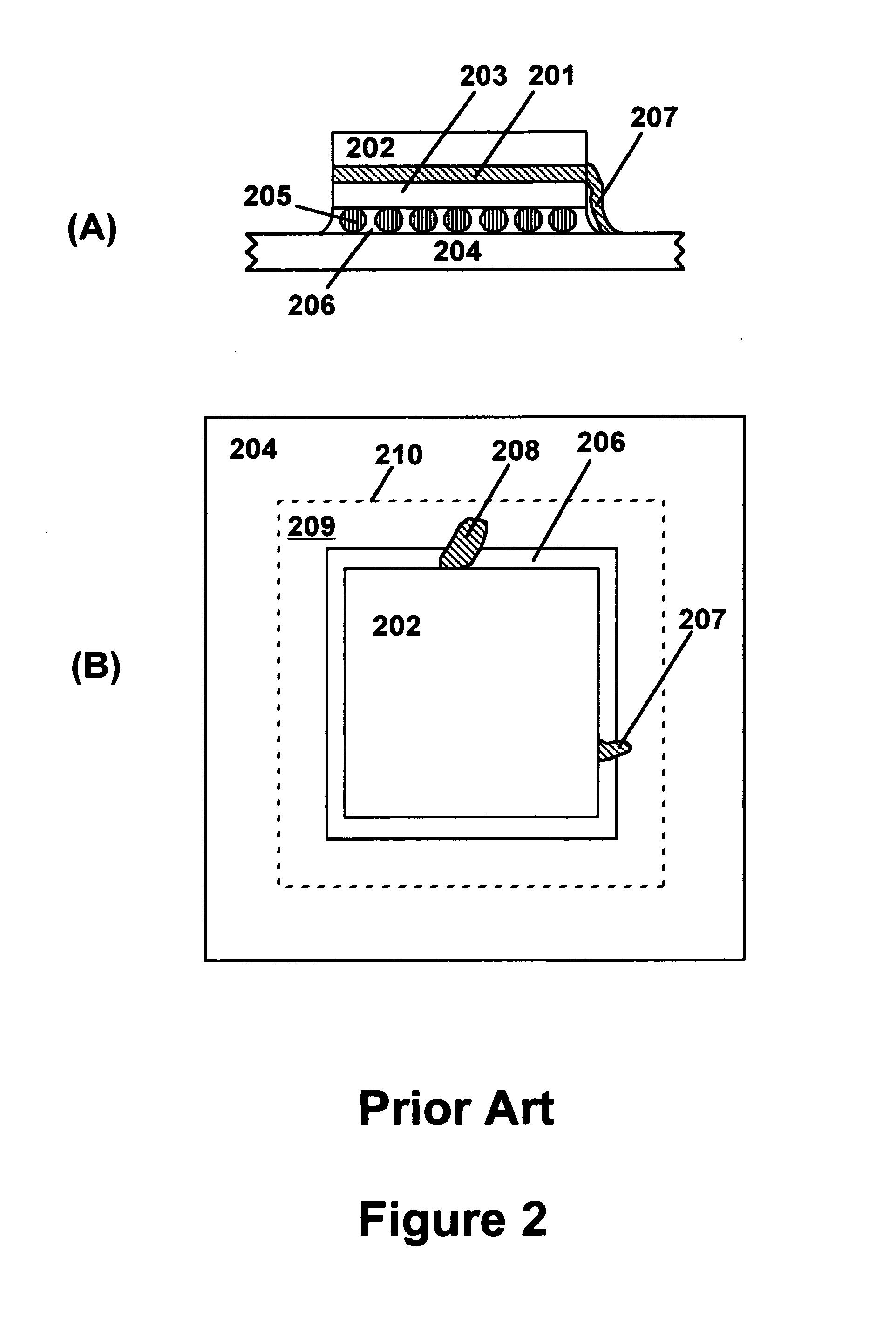
These prior art approaches to improving the performance of microelectronic thermal interfaces have the drawbacks that the liquid metal tends to be difficult to contain and is prone to oxidation that can lower the heat transfer efficiency.
These references teach that thermal interfaces involving solid materials are inefficient and unreliable.

Method used


Image

  • Microelectronic thermal interface
  • Microelectronic thermal interface
  • Microelectronic thermal interface

Examples


example 1

Feasibility Demonstration

[0052]A piece of 100×100 mesh copper screen (Dorstener Wire Technology) approximately 6×12 mm on the sides was placed on a ceramic coupon and one drop of Kester #186 RMA flux was added. Approximately half of the area of the copper screen was covered with a piece of indium foil that was 7 mils (0.2 mm) thick. When this assembly was placed on a hot plate set at 200° C., the indium foil reflowed and wet the copper screen well. A rigid metal plate was placed on the reflowed assembly and hit with a hammer to simulate a milling operation to smooth out observed unevenness in the reflowed indium surface. Micrometer measurements indicated that the uncoated portion of the copper screen was 9 mils thick, whereas the portion of the copper screen embedded in indium was 12 mils thick.

example 2

Simulated Thermal Interface Test

[0053]Formation of the interface of the invention was demonstrated using a test structure comprising rectangular pieces (1.0×1.5 cm) of a pure indium foil (9 mils thick) and a 100×100 mesh copper screen sandwiched between first and second coupons of FR-4 laminate material coated with an ENIG (electroless nickel immersion gold) coating. The procedure was as follows. An aliquot (5 μL) of Kester #186 RMA flux was pipetted onto the top of the first coupon. The piece of copper screen was placed on the fluxed surface of the first coupon, and the piece of indium foil was placed on the copper screen. An aliquot (5 μL) of Kester #186 RMA flux was pipetted onto the top of the indium foil. The second coupon was placed on top of the fluxed indium foil. This test structure, held together with a spring clip, was passed through a reflow oven having a four-minute temperature profile that peaked at 170° C. The reflowed indium wetted all solderable surfaces well, embed...

example 3

Pressure Embedded Copper Grid

[0054]The feasibility of pressing a metallic grid into a solder material to form the thermal interface of the invention was demonstrated using the test structure, soldering flux and reflow conditions of Example 2. In the present case, the copper screen was first treated in Kester #5520 Copper-Nu™ to remove surface oxides, and was then rinsed and dried. The deoxidized copper screen was then dipped in the soldering flux and dried in warm flowing air to remove flux volatile materials. This pre-fluxed copper screen was then pressed into the indium foil by roller milling to form a preform. An aliquot (5 μL) of Kester #186 RMA flux was pipetted onto both sides of the preform, which was then sandwiched between the first and second coupons. This test structure, held together with a spring clip, was passed through a reflow oven having a four-minute temperature profile that peaked at 170° C. The reflowed indium wetted all solderable surfaces well, embedding the co...


PUM

PropertyMeasurementUnit
angleaaaaaaaaaa
diameteraaaaaaaaaa
thickaaaaaaaaaa

Abstract

An improved thermal interface between an integrated circuit chip and a heat sink comprises a copper grid embedded in a layer of a solder material that has a fusion temperature higher than the maximum operating temperature of the semiconductor chip, and bonds to the semiconductor chip and the heat sink when heated to the fusion temperature of the solder material in the presence of a soldering flux. The copper grid has high thermal conductivity so that the amount of solder material needed for an efficient thermal interface is reduced and solder materials with less expensive components may be used. The copper grid also tends to mitigate local hot spots by enhancing lateral heat transfer, and inhibits solder spreading during formation of the thermal interface.

Description

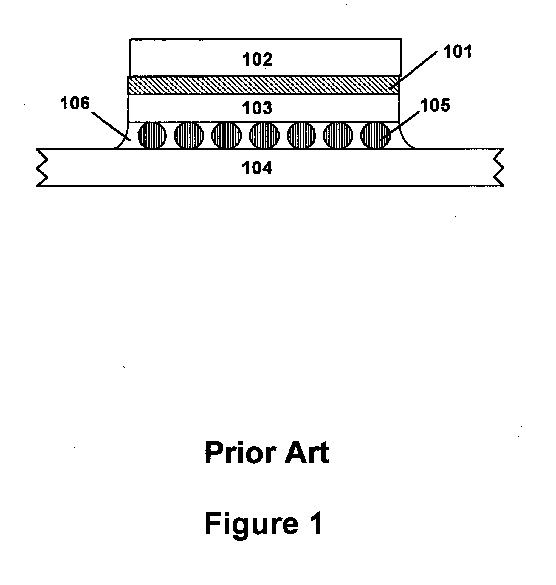
BACKGROUND OF THE INVENTION[0001]1. Field of the Invention[0002]This invention is concerned with microelectronic devices, and in particular with heat dissipation for integrated circuit (IC) chips.[0003]2. Description of the Related Art[0004]Modern microelectronic devices generally comprise integrated circuit (IC) chips that are electrically connected via a ball grid array on the chip bottom to a printed circuit board (or another substrate) by reflow soldering. For high-speed IC chips that generate a significant amount of heat during operation, the top of the chip is generally connected to a heat sink, which may comprise a heat radiator. A thin layer of a thermal interface material (TIM) is typically placed between the top of the chip and the heat sink to improve heat transfer. A typical TIM layer comprises a pure indium foil, which is reflowed to form an intimate bond between the chip and the heat sink so as to provide good heat transfer.[0005]As IC chips have decreased in size and ...

Claims


Application Information

Patent Timeline
Patent Type & Authority Applications(United States)
IPC IPC(8): H05K7/20F28F7/00B23K1/20B23K31/02
CPCH01L23/3733H01L23/42H01L23/433H01L2224/32245H01L2224/73253H01L2224/16225H01L2224/16227H01L2224/73204H01L2224/29076H01L2924/00014H01L2224/0401
Inventor DERAM, BRIAN
Owner KESTER
Learn More