Composite material for electric/electronic part, production method thereof, and electric/electronic part

Inactive Publication Date: 2011-04-21
FURUKAWA ELECTRIC CO LTD
View PDF3 Cites 3 Cited by
  • Summary
  • Abstract
  • Description
  • Claims
  • Application Information

AI Technical Summary

Benefits of technology

[0044]The composite material for an electric / electronic part of the present invention has very excellent adhesion between the resin film and the metal. The composite material has enhanced adhesion, and has satisfactory punchability and bending workability, by press working. Furthermore, when a composite material for an electric / electronic part is produced under the same conditions as in the present invention, there is a significant advantage that since the composite material is softer than the resin itself that has been completely cured, bending workability by press working is also enhanced, and working by pressing is made easier.
[0045]Furthermore, since the composite material for an electric / electronic part of the present invention has enhanced and excellent adhesion between the resin film and the metal, the composite material is also excellent in heat resistance, alkali resistance and the like; and since baking of the resin film is carried out in consideration of the post-treatments, the composite material sufficiently withstands a heat treatment or a post-plating treatment, both of which are post-treatments after working, and can be worked under the working conditions that are equivalent to those of an untreated material.

Problems solved by technology

However, in the case of the above-mentioned metal cases and the like, reduction of height is accompanied by reduction of internal volume; and there is a problem that insulation between the inner parts, terminals or wiring circuits and the electric / electronic part such as case, cover, cap or package (cover case) is not sufficiently assured.
Therefore, working into a desired shape becomes severe, and adhesion in various working process needs to be enhanced.
It is assumed that this gap is formed by insufficient adhesion between the metal base and the resin film.
As there is a practical limitation for reducing of the clearance in punching, it can be said that this tendency becomes increased as the above-mentioned worked piece is more miniaturized.
Besides, providing of the insulating film after fine working needs much time and effort and brings about cost increases, which is not practical.

Method used


Image

  • Composite material for electric/electronic part, production method thereof, and electric/electronic part
  • Composite material for electric/electronic part, production method thereof, and electric/electronic part
  • Composite material for electric/electronic part, production method thereof, and electric/electronic part

Examples


example 1

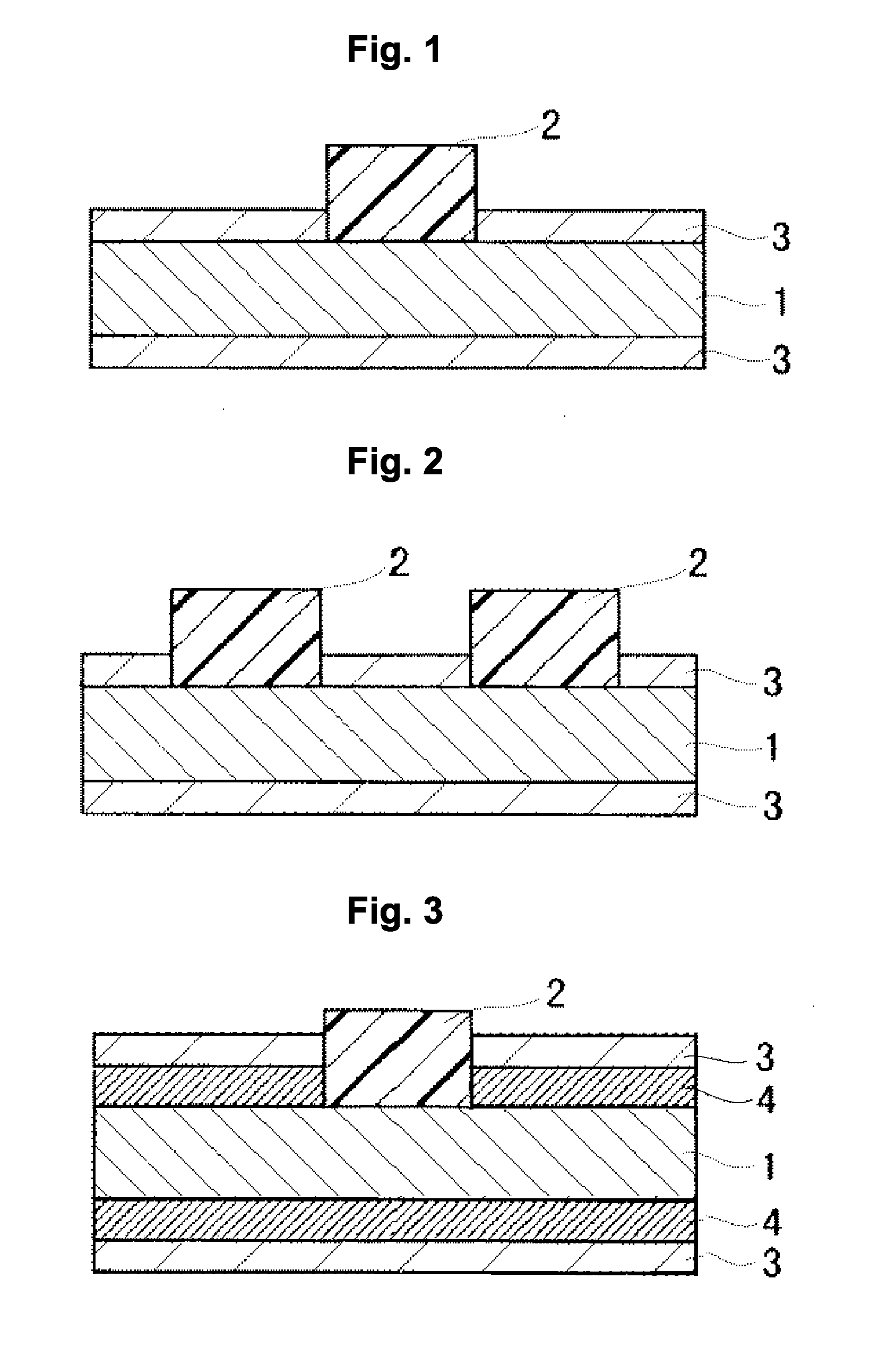
[0138]Strips of JIS alloy C5210R (phosphor bronze, manufactured by Furukawa Electric Co., Ltd.) having a thickness of 0.1 mm and a width of 20 mm were used as a metal base. The strips were subjected to electrolytic degreasing, acid pickling, water washing, and drying, in this order.

[0139]Then, a varnish (solid content: about 30%) containing a polyamide-imide (PAI) solution with N-methyl-2-pyrrolidone as a solvent was coated, on a center part in the width direction of the metal bases, at a coating thickness that would obtain a post-baking coating thickness of 10 μm (±1 μm), with a K-control coater (manufactured by RK Print Coat Instruments Ltd. UK), at a part of the metal bases, as illustrated in FIG. 1. Then, the predetermined heating treatment was performed, to dry the solvent and to cure, thereby to provide a resin film.

[0140]In Samples Nos. 101 to 905, the time for allowing the samples to stand in the furnace at a furnace temperature of 200° C. to 400° C. was varied, and the resi...


PUM

PropertyMeasurementUnit
Fractionaaaaaaaaaa
Fractionaaaaaaaaaa
Percent by massaaaaaaaaaa

Abstract

A composite material for an electric / electronic part, having a metal base, a resin film on at least a part of the metal base, and a layer of Sn or a Sn alloy on at least a part of the metal base at a site where the resin film is not provided, the layer of Sn or a Sn alloy including a solidified structure, and the resin film having a residual solvent quantity adjusted to 5% to 25% by mass.

Description

TECHNICAL FIELD[0001]The present invention relates to a composite material for an electric / electronic part having a resin film on a metal base. More particularly, the present invention relates to a composite material for an electric / electronic part having a resin film and a re-melted and solidified plating layer, on a metal base, an electric / electronic part using the composite material, and a method for producing the composite material.BACKGROUND ART[0002]On a printed circuit board of an electric / electronic device, separate elements, such as a ceramic oscillator, a crystal oscillator, a voltage controlled oscillator, a SAW filter, a diplexer, a coupler, a balun, an LPF, a BPF, and a dielectric duplexer; various modules each having a plurality of such elements integrated therein, such as an antenna switch module, a front end module, an RF integrated module, a radio communication module, an image sensor module, a tuner module, and a wireless LAN module; and parts such as a detection s...

Claims


Application Information

Patent Timeline
IPC IPC(8): B32B3/10B05D3/02
CPCC08G73/14Y10T428/12569C23C18/1605C23C18/1692C23C26/00C23C28/00C25D5/02C25D5/022C25D5/10C25D5/50C25D5/505H01R13/03H05K9/0084C23C28/023C23C28/021Y10T428/24917Y10T428/12396Y10T428/12229C09D179/08Y10T428/31685Y10T428/31681B32B15/08B32B15/088H01B17/62
Inventor TACHIBANA, AKIRASUGAHARA, CHIKAHITOKITAGAWA, SHUICHI
Owner FURUKAWA ELECTRIC CO LTD
Why Eureka
Try Eureka