Apparatus and method for solution coating thin layers

a technology of solution coating and apparatus, applied in the direction of vacuum evaporation coating, coating, cleaning using liquids, etc., can solve the problem of poor performance of electronic devices

Active Publication Date: 2011-04-14
LG CHEM LTD
View PDF17 Cites 6 Cited by
  • Summary
  • Abstract
  • Description
  • Claims
  • Application Information

AI Technical Summary

Benefits of technology

[0025]The vacuum system used in the above sequence utilizes a vacuum assist device (VAD) that creates a chamber around a selected station providing a pressure of less than one atmosphere. The combination of the VAD and slot die coater is referred to as a coating assembly. Sealing elements are used in conjunction with the coating assembly to produce the chamber having a designated pressure. The sealing elements provide a controlled leakage where the VAD approaches, but does not touch, the surface within the station (i.e. substrate, priming roll, etc.). In the cleaning station the VAD can remain in place with the slot die coater and vacuum to the VAD is off during the cleaning operation, alternatively, the VAD can be moved away from the slot die coater to accommodate cleaning of the slot die coater. After the cleaning operation a reverse flow of gas (air, nitrogen, etc.) can be sent through the VAD to remove any residual cleaning fluid. When sealing elements are working in conjunction with the coater assembly, a vacuum source of the VAD may be any source of vacuum, such as a blower, pump, evacuated tank or any known means of providing sub-ambient pressure.

Problems solved by technology

Viscous drag forces are one factor in removing solution from the gap, leading to non-uniform deposition of the layers and resultant poor performance in an electronic device.

Method used


Image

  • Apparatus and method for solution coating thin layers
  • Apparatus and method for solution coating thin layers
  • Apparatus and method for solution coating thin layers

Examples


Embodiment Construction

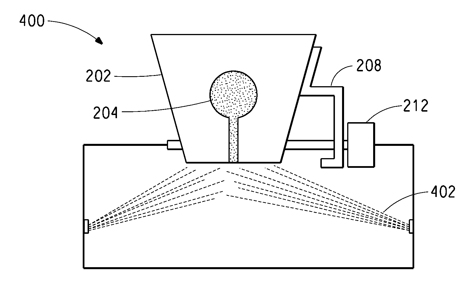
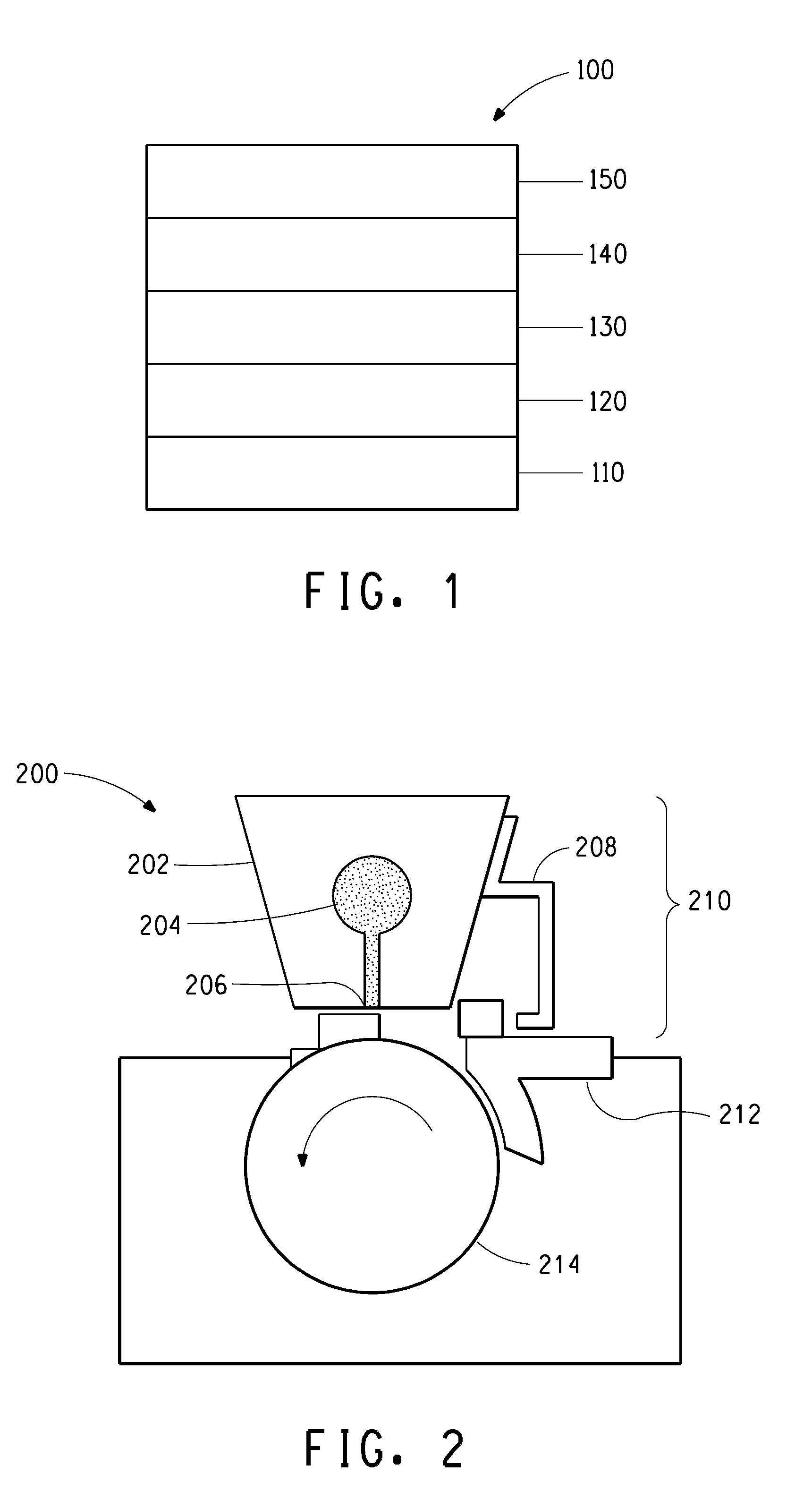
[0032]One example of an electronic device comprising an organic light-emitting diode (“OLED”), as shown in FIG. 1 and designated 100. The device has an anode layer 110, a buffer layer 120, a photoactive layer 130, and a cathode layer 150. Adjacent to the cathode layer 150 is an optional electron-injection / transport layer 140. Between the buffer layer 120 and the photoactive layer 130, is an optional hole-injection / transport layer (not shown).

[0033]As used herein, the term “buffer layer” or “buffer material” is intended to mean electrically conductive or semiconductive materials and may have one or more functions in an organic electronic device, including but not limited to, planarization of the underlying layer, charge transport and / or charge injection properties, scavenging of impurities such as oxygen or metal ions, and other aspects to facilitate or to improve the performance of the organic electronic device. Buffer materials may be polymers, oligomers, or small molecules, and ma...


PUM

PropertyMeasurementUnit
slot widthaaaaaaaaaa
distanceaaaaaaaaaa

Abstract

An apparatus and method for solution coating layers onto a substrate of an electronic device. A slot die coater in conjunction with a vacuum assist device is used in priming, coating and cleaning stations to produce thin layers having performance advantages over competing technologies.

Description

FIELD OF THE DISCLOSURE[0001]This disclosure relates in general to a process for making an electronic device. In particular, it relates to a method and apparatus for solution coating layers using a slot die coater in conjunction with a vacuum assist device.BACKGROUND INFORMATION[0002]Increasingly, active organic molecules are used in electronic devices. These active organic molecules have electronic or electro-radiative properties including electroluminescence. Electronic devices that incorporate organic active materials may be used to convert electrical energy into radiation and may include a light-emitting diode, light-emitting diode display, or diode laser.[0003]Two methods are commonly used to prepare organic light-emitting diode (“OLED”) displays: vacuum deposition, and solution processing. (The latter includes all forms of applying the layers from a fluid, as a true solution or a suspension.) Vacuum deposition equipment typically has very high investment costs, and inferior ma...

Claims


Application Information

Patent Timeline
Patent Type & Authority Applications(United States)
IPC IPC(8): B05D1/26B05C5/02B08B3/00
CPCB05B15/0258B05C5/0254H01L51/56H01L51/0003H01L51/0004B05D3/0493B05B15/555H10K71/12H10K71/13H10K71/00
Inventor LANG, CHARLES D.FAIRCLOTH, TAMI JANENE
Owner LG CHEM LTD
Why Eureka
Try Eureka