Thin-film transistor array, method of fabricating the same, and liquid crystal display device including the same
a technology of thin-film transistors and liquid crystal displays, which is applied in the direction of semiconductor devices, electrical equipment, instruments, etc., can solve the problems of unavoidable a number and increase of photolithography steps, and achieve the effect of enhancing reliability in electrical connections
- Summary
- Abstract
- Description
- Claims
- Application Information
AI Technical Summary
Benefits of technology
Problems solved by technology
Method used
Image
Examples
first exemplary embodiment
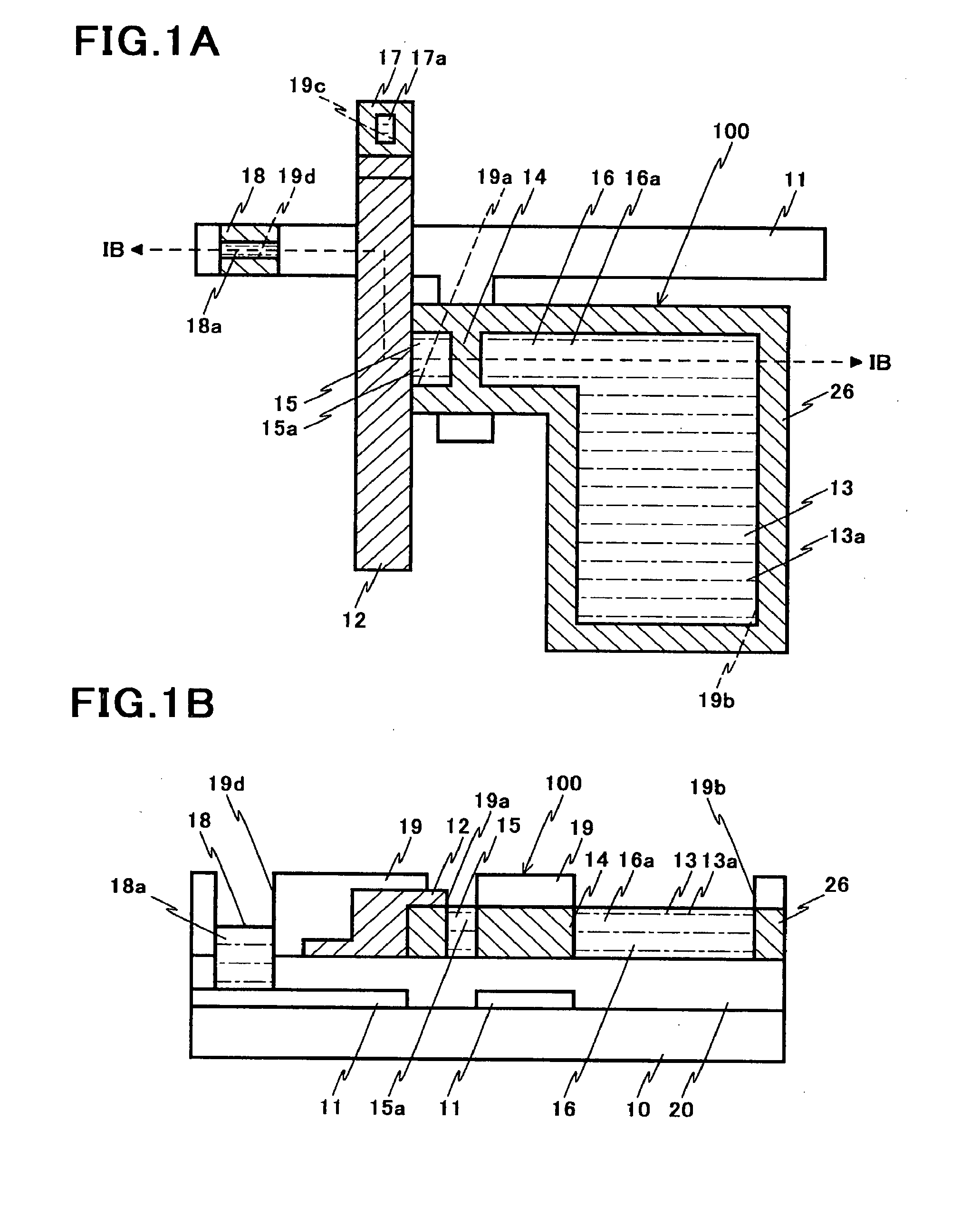
[0067]FIG. 1A is a plain view of a thin-film transistor array in accordance with the first exemplary embodiment, and FIG. 1B is a cross-sectional view taken along the line IB-IB in FIG. 1A.
[0068]The thin-film transistor array in accordance with the first exemplary embodiment is a bottom gate stagger type thin-film transistor array.
[0069]The thin-film transistor array in accordance with the first exemplary embodiment is designed to include a plurality of thin-film transistors 100 arranged in a matrix on an electrically insulating substrate 10, that is, the thin-film transistors 100 are arranged on the electrically insulating substrate 10 in both a column direction (for instance, an up-down direction in FIG. 1A) and a row direction which is perpendicular to the column direction in a plane in which the column direction lies (for instance, a left-right direction in FIG. 1A).
[0070]For simplification, FIGS. 1A and 1B illustrate only one thin-film transistor 100 and a structure existing ar...
second exemplary embodiment
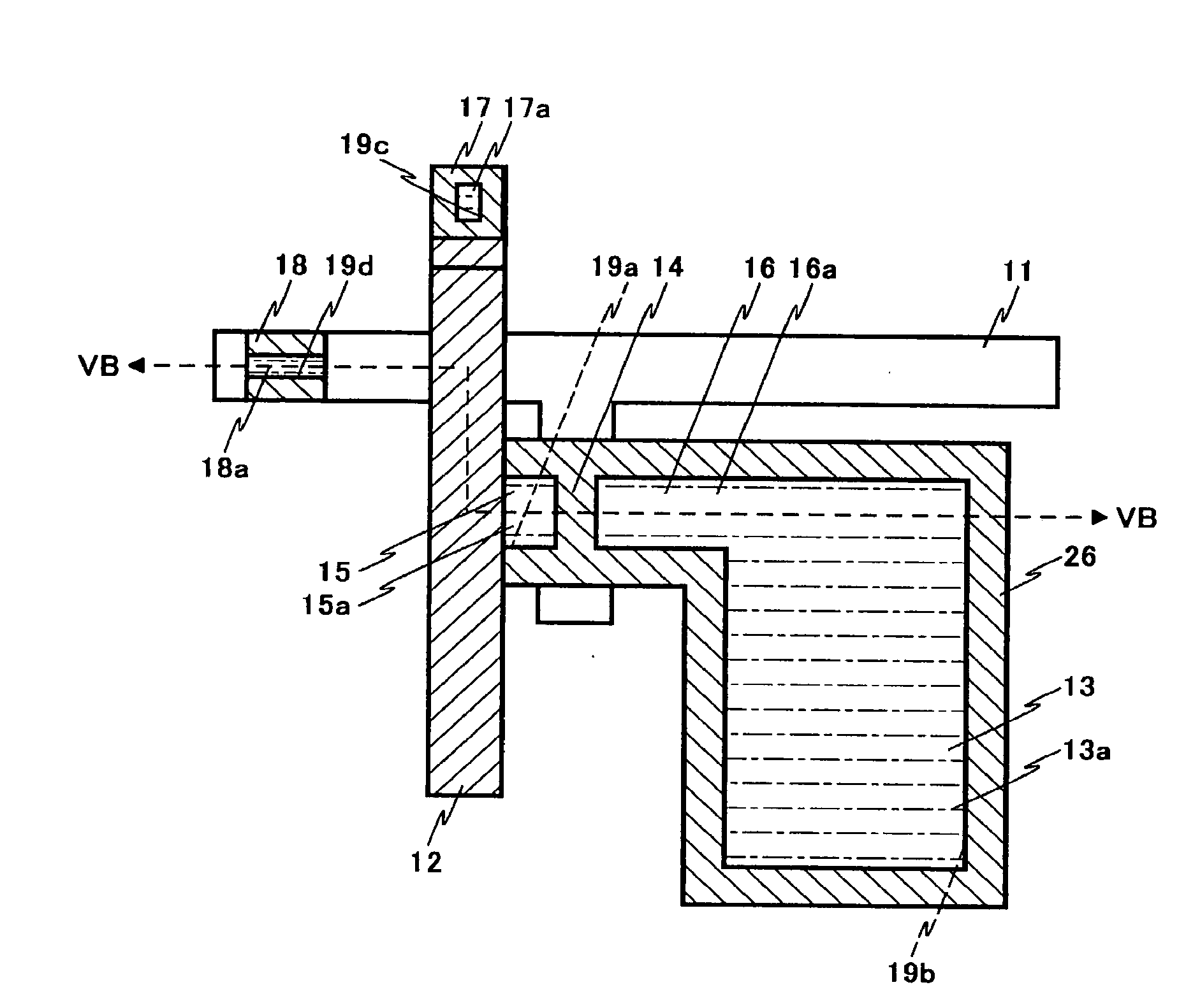
[0124]Hereinbelow is explained a method of a thin-film transistor array in accordance with the second exemplary embodiment, with reference to FIGS. 6A to 9B.
[0125]The thin-film transistor array in accordance with the second exemplary embodiment is of a bottom gate planar type.
[0126]FIGS. 6A, 7A, 8A and 9A are plain views showing respective steps to be carried out in a method of fabricating the thin-film transistor array in accordance with the second exemplary embodiment, and FIGS. 6B, 7B, 8B and 9B are cross-sectional views taken along the lines VIB-VIB, VIIB-VIIB, VIIIB-VIIIB, and IXB-IXB, respectively.
[0127]Parts or elements in the second exemplary embodiment that correspond to those of the first exemplary embodiment have been provided with the same reference numerals.
[0128]First, as illustrated in FIGS. 6A and 6B, a gate metal film (defined as “an electrically conductive film” in claims) is formed on the electrically insulating substrate 10. For instance, the gate metal film is c...
third exemplary embodiment
[0147]Hereinbelow is explained a method of a thin-film transistor array in accordance with the third exemplary embodiment, with reference to FIGS. 10A to 13B.
[0148]The thin-film transistor array in accordance with the third exemplary embodiment is of a top gate planar type.
[0149]FIGS. 10A, 11A, 12A and 13A are plain views showing respective steps to be carried out in a method of fabricating the thin-film transistor array in accordance with the third exemplary embodiment, and FIGS. 10B, 11B, 12B and 13B are cross-sectional views taken along the lines XB-XB, XIB-XIB, XIIB-XIIB, and XIIIB-XIIIB, respectively.
[0150]Parts or elements in the third exemplary embodiment that correspond to those of the first exemplary embodiment have been provided with the same reference numerals.
[0151]First, as illustrated in FIGS. 10A and 10B, an amorphous ZnO film is formed by sputtering at room temperature on the electrically insulating substrate 10. The electrically insulating substrate 10 is comprised ...
PUM
 Abstract
Description
Claims
Application Information
 - R&D
- Intellectual Property
- Life Sciences
- Materials
- Tech Scout
- Unparalleled Data Quality
- Higher Quality Content
- 60% Fewer Hallucinations
Browse by: Latest US Patents, China's latest patents, Technical Efficacy Thesaurus, Application Domain, Technology Topic, Popular Technical Reports.
© 2025 PatSnap. All rights reserved.Legal|Privacy policy|Modern Slavery Act Transparency Statement|Sitemap|About US| Contact US: help@patsnap.com


