
LONG WAVELENGTH NONPOLAR AND SEMIPOLAR (Al,Ga,In)N BASED LASER DIODES

a laser diode and long wavelength technology, applied in the field of laser diodes, can solve the problems of low slope efficiency and miscut device results, and achieve the effects of reducing waveguide scattering, improving structural, electrical and optical properties of long wavelength lds, and maintaining smooth surface morphology

Inactive Publication Date: 2010-12-09
RGT UNIV OF CALIFORNIA
View PDF70 Cites 295 Cited by
  • Summary
  • Abstract
  • Description
  • Claims
  • Application Information

AI Technical Summary

Benefits of technology

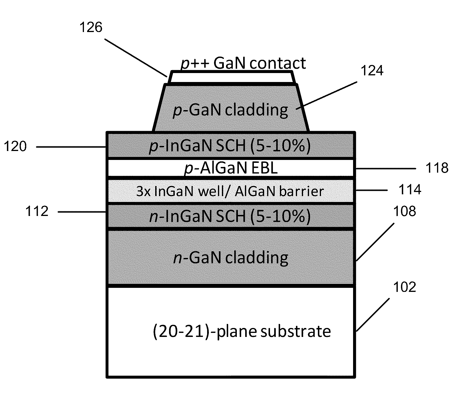
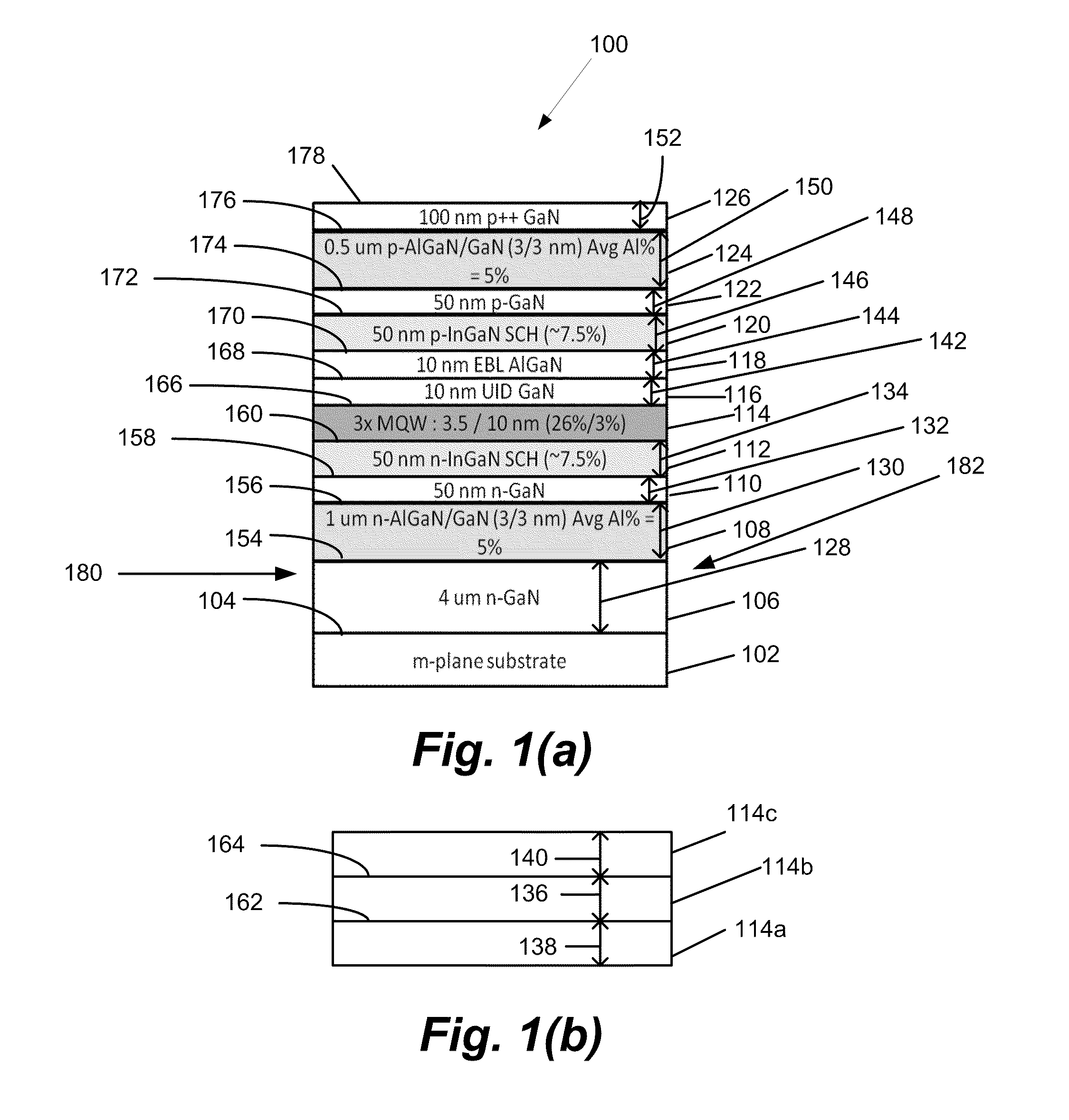
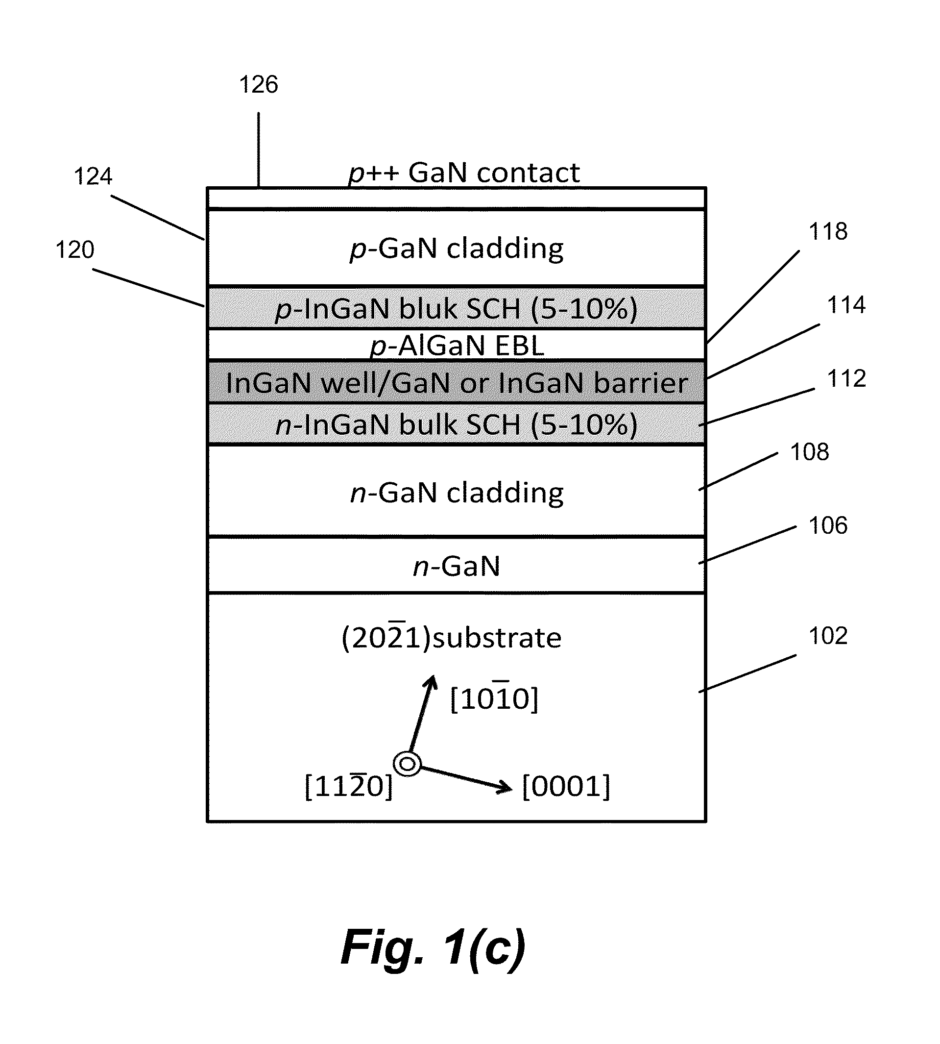
[0019]To overcome the limitations in the prior art described above, and to overcome other limitations that will become apparent upon reading and understanding the present specification, the present invention describes techniques to fabricate long wavelength laser diodes (LDs) employing nonpolar and semipolar InGaN / GaN based active regions. The invention features novel structure and epitaxial growth techniques to improve structural, electrical and optical properties of long wavelength LDs, especially in the blue-green spectral range. Some of the key features include using miscut substrates and unconventional growth conditions in order to maintain smooth surface morphology, reduce waveguide scattering, and use of novel growth techniques to lower p-GaN contact resistance.
[0021]The method may further comprise using 100% nitrogen carrier gas at atmospheric pressure to grow the one or more device layers on the off-axis surface of the substrate, resulting in the device layers having smooth surface morphology free of pyramidal hillocks observed in device layers grown on nominally on-axis m-plane GaN substrates. The device layers grown using the nitrogen carrier gas at atmospheric pressure may comprise all of the LD structure's n-type layers, including the silicon-doped n-type AlGaN / GaN superlattice, resulting in smooth interfaces and excellent structural properties for the LD structure, as compared to device layers grown without using 100% nitrogen carrier gas.
[0023]The method may further comprise growing the quantum wells at a first temperature and with an Indium content so that the quantum wells emit green light, wherein the first growth rate maintains smooth interfaces and prevents faceting as compared to the quantum wells grown at a different growth rate.
[0024]Each of the quantum wells may be between quantum well barriers to form a light emitting active region, and the method may further comprise growing the quantum well barriers at a second growth rate slower than the first growth rate, resulting in smooth surface morphology and interfaces for the device layers, including the quantum wells, grown on the quantum well barriers, as compared to the barriers grown at a different faster growth rate, for example.
[0026]High Indium content InxGa1-xN separate confinement heterostructure (SCH) layers may be on either side of the active region and the electron blocking layer, with x>7%, and the method may further comprising growing the SCH layers at (1) a third temperature higher temperature than a temperature used to grow other layers in the LD structure, (2) a slower growth rate of more than 0.3 Angstroms per second and less than 0.7 Angstroms per second, and (3) a high Trimethylindium / Triethylgallium (TEG) ratio of greater than 1.1, resulting in a smooth and defect free wave-guiding layer.

Problems solved by technology

LDs emitting beyond the blue spectral region have also been reported based on c-plane technology, but the slope efficiency was low due to QCSE-related low internal efficiency and high mirror reflectivities [11-12].
To date, very few groups have reported device results based on miscut m-plane GaN substrates.

Method used


Image

  • LONG WAVELENGTH NONPOLAR AND SEMIPOLAR (Al,Ga,In)N BASED LASER DIODES
  • LONG WAVELENGTH NONPOLAR AND SEMIPOLAR (Al,Ga,In)N BASED LASER DIODES
  • LONG WAVELENGTH NONPOLAR AND SEMIPOLAR (Al,Ga,In)N BASED LASER DIODES

Examples


Embodiment Construction

[0056]In the following description of the preferred embodiment, reference is made to the accompanying drawings which form a part hereof, and in which is shown by way of illustration a specific embodiment in which the invention may be practiced. It is to be understood that other embodiments may be utilized and structural changes may be made without departing from the scope of the present invention.

[0057]Nomenclature

[0058]GaN and its ternary and quaternary compounds incorporating aluminum and indium (AlGaN, InGaN, AlInGaN) are commonly referred to using the terms (Al,Ga,In)N, III-nitride, Group III-nitride, nitride, Al(1-x-y)InyGaxN where 0<x<1 and 0<y<1, or AlInGaN, as used herein. All these terms are intended to be equivalent and broadly construed to include respective nitrides of the single species, Al, Ga, and In, as well as binary, ternary and quaternary compositions of such Group III metal species. Accordingly, these terms comprehend the compounds AlN, GaN, and InN, as well as t...


PUM


Abstract

A laser diode, grown on a miscut nonpolar or semipolar substrate, with lower threshold current density and longer stimulated emission wavelength, compared to conventional laser diode structures, wherein the laser diode's (1) n-type layers are grown in a nitrogen carrier gas, (2) quantum well layers and barrier layers are grown at a slower growth rate as compared to other device layers (enabling growth of the p-type layers at higher temperature), (3) high Al content electron blocking layer enables growth of layers above the active region at a higher temperature, and (4) asymmetric AlGaN SPSLS allowed growth of high Al containing p-AlGaN layers. Various other techniques were used to improve the conductivity of the p-type layers and minimize the contact resistance of the contact layer.

Description

CROSS-REFERENCE TO RELATED APPLICATIONS[0001]This application claims the benefit under 35 U.S.C. Section 119(e) of co-pending and commonly assigned U.S. Provisional Patent Application Ser. No. 61 / 184,729, filed on Jun. 5, 2009, by Arpan Chakraborty, You-Da Lin, Shuji Nakamura, and Steven P. DenBaars, entitled “LONG WAVELENGTH m-PLANE (Al,Ga,In)N BASED LASER DIODES” attorney's docket number 30794.315-US-P1 (2009-616-1);[0002]which application is incorporated by reference herein.[0003]This application is related to the following co-pending and commonly-assigned U.S. Patent Applications:[0004]Utility application Ser. No. 12 / 716,176, filed on Mar. 2, 2010, by Robert M. Farrell, Michael Iza, James S. Speck, Steven P. DenBaars, and Shuji Nakamura, entitled “METHOD OF IMPROVING SURFACE MORPHOLOGY OF (Ga,Al,In,B)N THIN FILMS AND DEVICES GROWN ON NONPOLAR OR SEMIPOLAR (Ga,Al,In,B)N SUBSTRATES,” attorneys' docket number 30794.306-US-U1 (2009-429-1), which application claims the benefit under ...

Claims


Application Information

Patent Timeline
IPC IPC(8): H01S5/00H01L21/20
CPCB82Y20/00H01S5/2022H01S5/34333H01S5/3213H01S5/3216H01S5/3202H01S5/2009H01S5/2031H01S5/22H01S5/320275
Inventor CHAKRABORTY, ARPANLIN, YOU-DANAKAMURA, SHUJIDENBAARS, STEVEN P.
Owner RGT UNIV OF CALIFORNIA
Learn More