
Semiconductor thin film, semiconductor thin film manufacturing method and semiconductor element

a technology of semiconductor thin film and semiconductor elements, applied in the field of semiconductor thin film, can solve the problems of low thermal stability, no advantages in forming a film at low temperature, and the change of semiconductor properties, so as to achieve stable semiconductor properties, hardly impaired semiconductor properties, and easy oxidation

Inactive Publication Date: 2010-05-27
IDEMITSU KOSAN CO LTD
View PDF3 Cites 15 Cited by
  • Summary
  • Abstract
  • Description
  • Claims
  • Application Information

AI Technical Summary

Benefits of technology

[0014]In addition, oxygen that is thermally fixed in an amorphous structure is easily liberated. For instance, when a semiconductor thin film is heated under vacuum, oxygen vacancy occurs due to the liberation of oxygen. Then, carriers are increased and thus the semiconductor properties may be impaired.
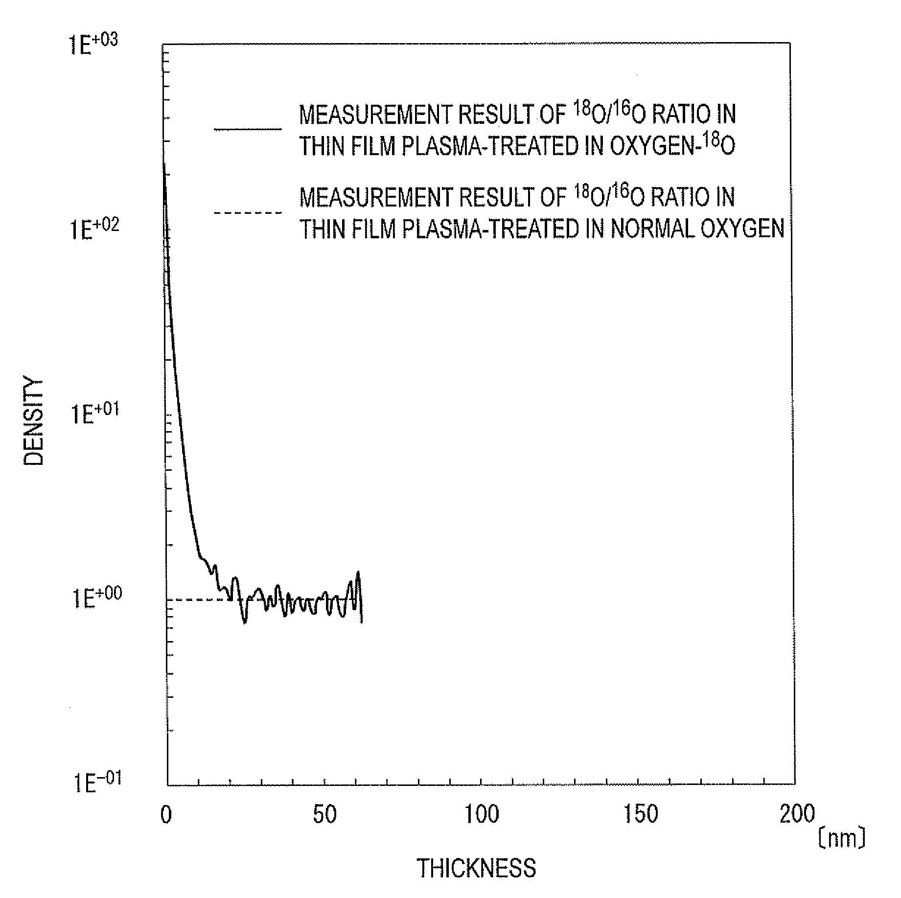
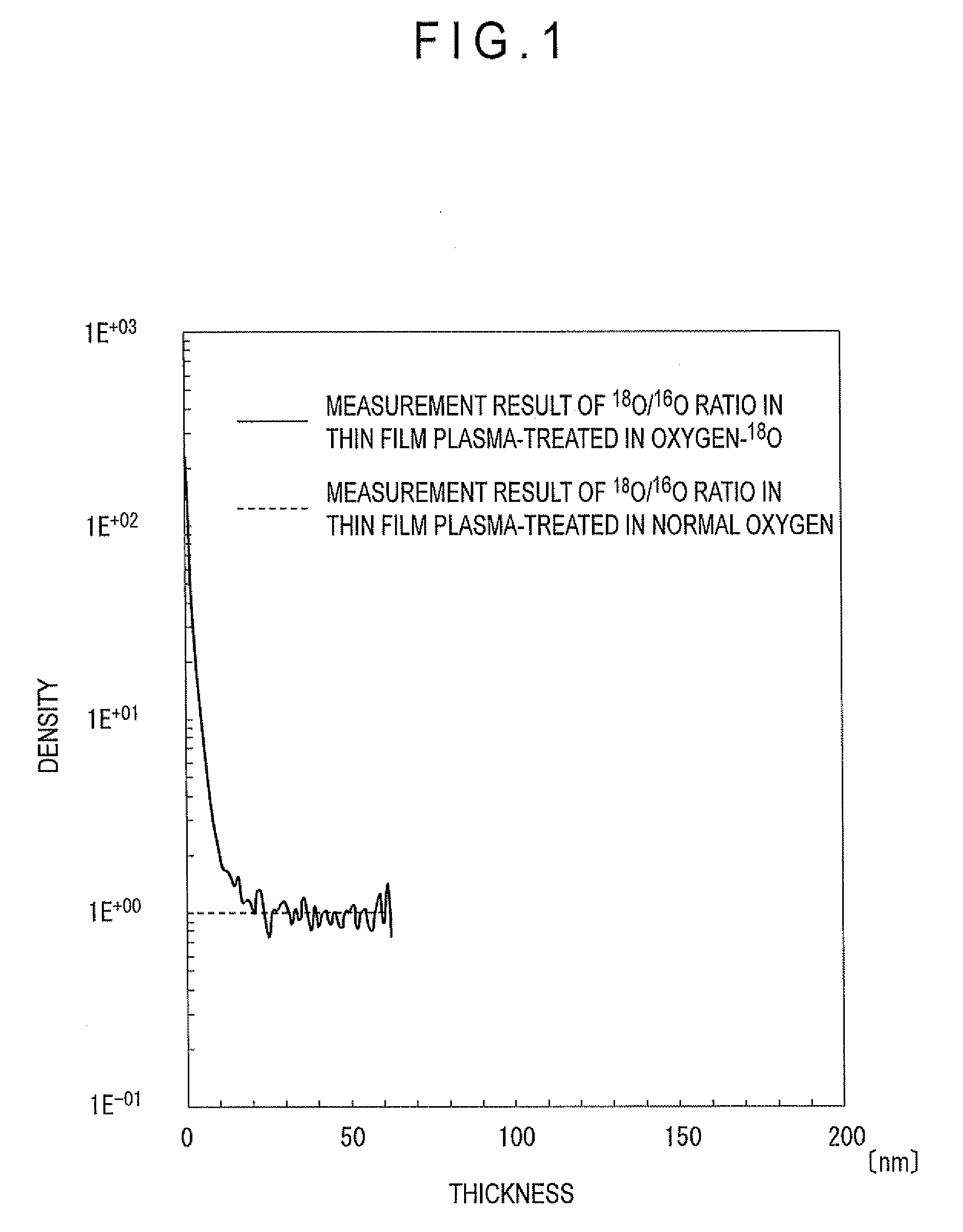
[0090]In addition, a semiconductor thin film having low carrier density can be efficiently manufactured because the oxygen vacancy can be reduced by the oxygen plasma. Further, because the temperature of a substrate can be maintained at low temperature of 200 degrees C. or less by using the plasma, the semiconductor thin film can be formed on a substrate of low heat resistance such as a film.

Problems solved by technology

However, since the oxide film formed in the oxygen atmosphere as disclosed in Patent Documents 1 to 7 is formed of amorphous oxide, its thermal stability is low and its semiconductor properties may change due to prolonged energization.
However, as far as heating is required, there are no advantages in forming a film at low temperature by utilizing amorphous properties.
Then, carriers are increased and thus the semiconductor properties may be impaired.
Thus, when the conditions for generating the oxygen-containing plasma are not appropriate, the semiconductor properties of the semiconductor thin film as the oxide film may be impaired by irradiation of the oxygen-containing plasma.

Method used


Image

  • Semiconductor thin film, semiconductor thin film manufacturing method and semiconductor element
  • Semiconductor thin film, semiconductor thin film manufacturing method and semiconductor element
  • Semiconductor thin film, semiconductor thin film manufacturing method and semiconductor element

Examples


examples

[0202]The above-described embodiments will be described in further detail below with reference to Examples and Comparatives. It should be noted that the invention is not limited to Examples at all.

examples of first exemplary embodiment

Comparative 1-1

[0203]With the use of an RF (radio frequency) magnetron sputtering apparatus (manufactured by SHIMADZU CORPORATION, brand name: HMS-552), an indium oxide-gallium oxide-zinc oxide (IGZO) thin film having thickness of 100 nm was formed on a glass by sputtering at room temperature in the presence of argon gas.

[0204]A target (manufactured by Idemitsu Kosan Co., Ltd.) was made of indium oxide, gallium oxide and zinc oxide (molar ratio of In:Ga:Zn=1:1:1).

example 1-1

[0205]The IGZO thin film obtained in Comparative 1-1 was exposed for 10 minutes to an oxygen plasma generated under the condition that frequency was 13.56 MHz, amplifier power was 500 W and oxygen pressure was 330 Pa. During this plasma treatment, the temperature of a substrate was less than 120 degrees C.

Evaluation of IGZO Thin Films of Example 1-1 and Comparative 1-1

[0206]X-ray diffraction was conducted on the IGZO thin film as an amorphous oxide thin film obtained in Comparative 1-1 and the IGZO thin film exposed to the oxygen plasma obtained in Example 1-1. The thin film obtained in Comparative 1-1 was amorphous because an X-ray diffraction peak was not observed. The IGZO thin film exposed to the oxygen plasma obtained in Example 1-1 was also amorphous because an X-ray diffraction peak was not observed.

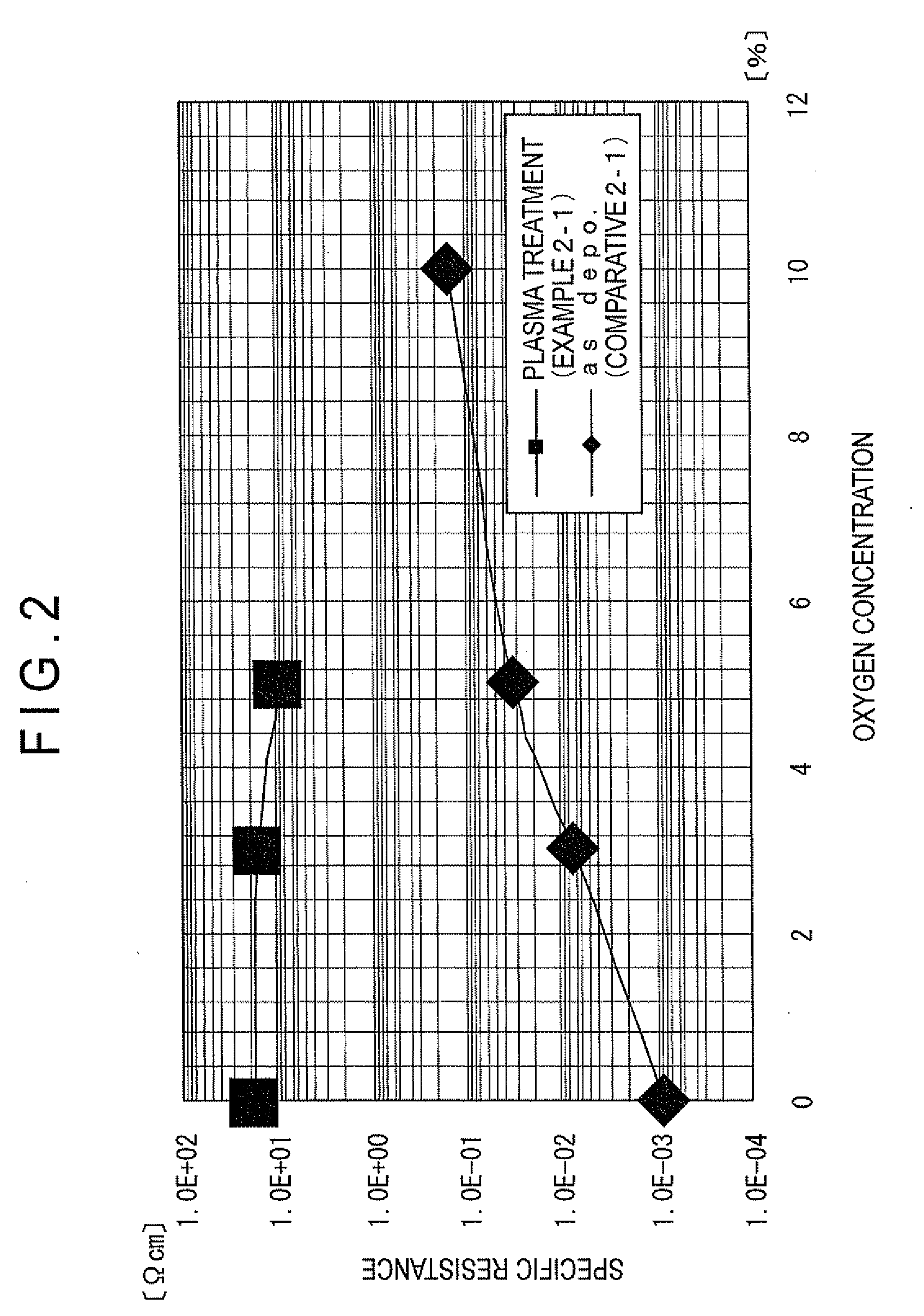
[0207]Table 1 shows specific resistances of the IGZO thin film of Example 1-1 and the IGZO thin film of Comparative 1-1.

[0208]The IGZO thin film of Example 1-1 had a specific resi...


PUM

PropertyMeasurementUnit
frequencyaaaaaaaaaa
frequencyaaaaaaaaaa
pressureaaaaaaaaaa

Abstract

An amorphous oxide thin film containing amorphous oxide is exposed to an oxygen plasma generated by exciting an oxygen-containing gas in high frequency. The oxygen plasma is preferably generated under the condition that applied frequency is 1 kHz or more and 300 MHz or less and pressure is 5 Pa or more. The amorphous oxide thin film is preferably exposed by a sputtering method, ion-plating method, vacuum deposition method, sol-gel method or fine particle application method.

Description

TECHNICAL FIELD[0001]The present invention relates to a semiconductor thin film, a manufacturing method thereof and a semiconductor device therewith. More particularly, the present invention relates to a semiconductor thin film obtained by exposing a thin film containing amorphous oxide to an oxygen plasma, a manufacturing method thereof and a semiconductor device therewith.BACKGROUND ART[0002]As semiconductors for use in transistors or the like, semiconductor thin films containing oxide such as indium oxide, gallium oxide and tin oxide have been traditionally known. Such a semiconductor thin film can be formed at low temperature as compared to a semiconductor such as silicon. Thus, a device having a substrate made of a heat-labile resin material can be designed (for instance, see Patent Documents 1 to 7).[0003]Patent Documents 1 to 7 disclose that: an oxide film for use as a semiconductor thin film is formed of amorphous oxide that contains, for instance, indium, zinc and gallium; ...

Claims


Application Information

Patent Timeline
Patent Type & Authority Applications(United States)
IPC IPC(8): H01L29/22H01L21/34
CPCC01G9/02C23C14/58C01G15/006C01G19/006C01G19/02C01P2002/50C01P2002/72C01P2006/40C23C14/086C23C14/5826C23C14/5853H01L21/02554H01L21/02565H01L21/02573H01L21/02581H01L21/02592H01L21/02631C03C17/23C23C14/08C01G15/00C03C17/245C03C17/2453C03C2217/215C03C2217/23C03C2217/231C03C2217/24C03C2217/944C03C2217/948C03C2218/156C03C2218/32C01B13/14
Inventor INOUE, KAZUYOSHIUTSUNO, FUTOSHIHONDA, KATSUNORI
Owner IDEMITSU KOSAN CO LTD
Learn More