Wireless IC device and component for wireless IC device
a wireless ic chip and wireless technology, applied in the field of wireless ic devices, can solve the problem of extreme difficulty in mounting the wireless ic chip b>310, and achieve the effect of stable frequency properties
- Summary
- Abstract
- Description
- Claims
- Application Information
AI Technical Summary
Benefits of technology
Problems solved by technology
Method used
Image
Examples
first preferred embodiment
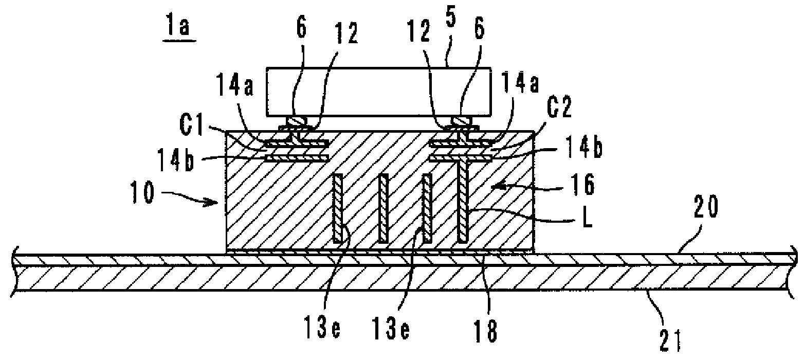
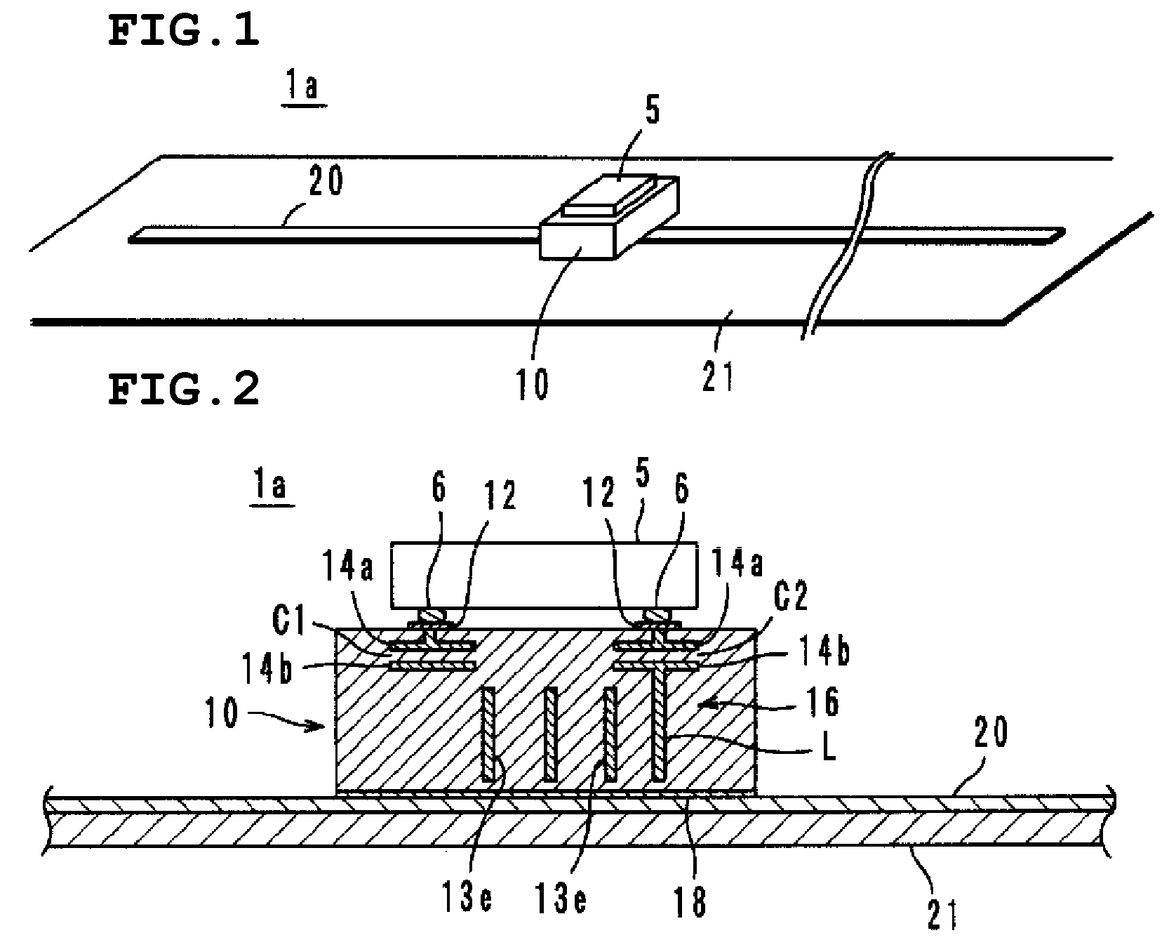
[0104]A wireless IC device 1a according to the first preferred embodiment is a monopole type, as illustrated in FIG. 1 and FIG. 2, and includes a wireless IC chip 5, a power supply circuit board 10 mounted on the wireless IC chip 5, and a radiation pattern 20 bonding the power supply circuit board 10. The wireless IC chip 5 includes a clock circuit, a logic circuit, and a memory circuit, stores necessary information therein, and is subjected to direct DC connection with a power supply circuit 16 provided in the power supply circuit board 10.
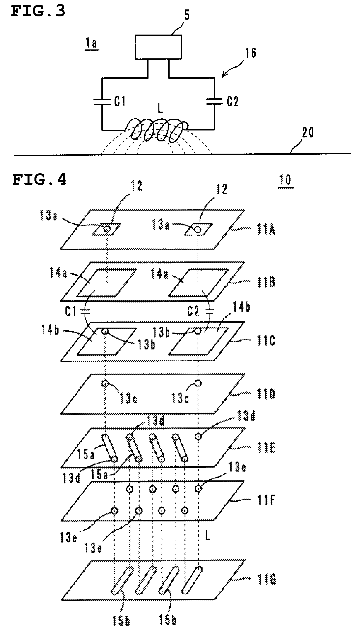
[0105]The power supply circuit 16 is a circuit for supplying a transmission signal having a predetermined frequency to the radiation pattern 20, and / or a circuit for selecting a reception signal having a predetermined frequency from signals received at the radiation pattern 20, and supplying it to the wireless IC chip 5, and includes a resonant circuit for resonating with the frequency of a transmission / reception signal.
[0106]As illustrated in FI...
second preferred embodiment
[0120]A wireless IC device 1b according to a second preferred embodiment is obtained by branching the radiation pattern 20 ninety degrees as shown in FIG. 8. That is to say, the radiation pattern 20 includes a radiation portion 20a extending in the X-axis direction within an x-y plane, and a radiation portion 20b extending in the Y-axis direction, a portion above the extension of the radiation portion 20a defines a power supply portion 20d, and the power supply circuit board 10, on which the wireless IC chip 5 is mounted, is adhered to the power supply portion 20d.
[0121]Note that the internal configuration of the power supply circuit board 10 is preferably the same as that in the first preferred embodiment, and the operations and advantages of the present second preferred embodiment are substantially the same as those in the first preferred embodiment. Further, the radiation portions 20a and 20b extend in the X-axis direction and Y-axis direction, whereby circularly-polarized waves...
third preferred embodiment
[0122]With a wireless IC device 1c according to a third preferred embodiment, as illustrated in FIGS. 9A and 9B, the radiation pattern 20 includes radiation portions 20a, 20b, and 20c extending in the X-axis direction, Y-axis direction, and Z-axis direction in x-y-z space, a portion above the extension of the radiation portion 20a defines a power supply portion 20d, and the power supply circuit board 10, on which the wireless IC chip 5 is mounted, is adhered to the power supply portion 20d.
[0123]The radiation pattern 20 of this wireless IC device 1c is adhered to a corner portion of a box-shaped article, the radiation portions 20a, 20b, and 20c extending three-dimensionally, so the directivity of the antenna is eliminated, and consequently, effective transmission / reception can be performed in any direction. Further, the other operations and advantages of the wireless IC device 1c are the same as those in the first preferred embodiment.
PUM
 Abstract
Description
Claims
Application Information
 - R&D
- Intellectual Property
- Life Sciences
- Materials
- Tech Scout
- Unparalleled Data Quality
- Higher Quality Content
- 60% Fewer Hallucinations
Browse by: Latest US Patents, China's latest patents, Technical Efficacy Thesaurus, Application Domain, Technology Topic, Popular Technical Reports.
© 2025 PatSnap. All rights reserved.Legal|Privacy policy|Modern Slavery Act Transparency Statement|Sitemap|About US| Contact US: help@patsnap.com


