
Electrically-driven optical proximity correction to compensate for non-optical effects

a non-optical effect, electrically driven technology, applied in the direction of photomechanical equipment, stochastic cad, instruments, etc., can solve the problems of increasing the number of cells, increasing the cost of equipment, and requiring complicated connections between cells,

Active Publication Date: 2010-05-13
SIEMENS PROD LIFECYCLE MANAGEMENT SOFTWARE INC
View PDF4 Cites 42 Cited by
  • Summary
  • Abstract
  • Description
  • Claims
  • Application Information

AI Technical Summary

Benefits of technology

[0011]It is therefore one object of the present invention to provide an improved method of converting of an integrated circuit design into a geometric layout for semiconductor wafer fabrication.
[0013]It is yet another object of the present invention to provide a method of generating a pattern mask for a layer of an integrated circuit design which compensates for such non-optical variations.
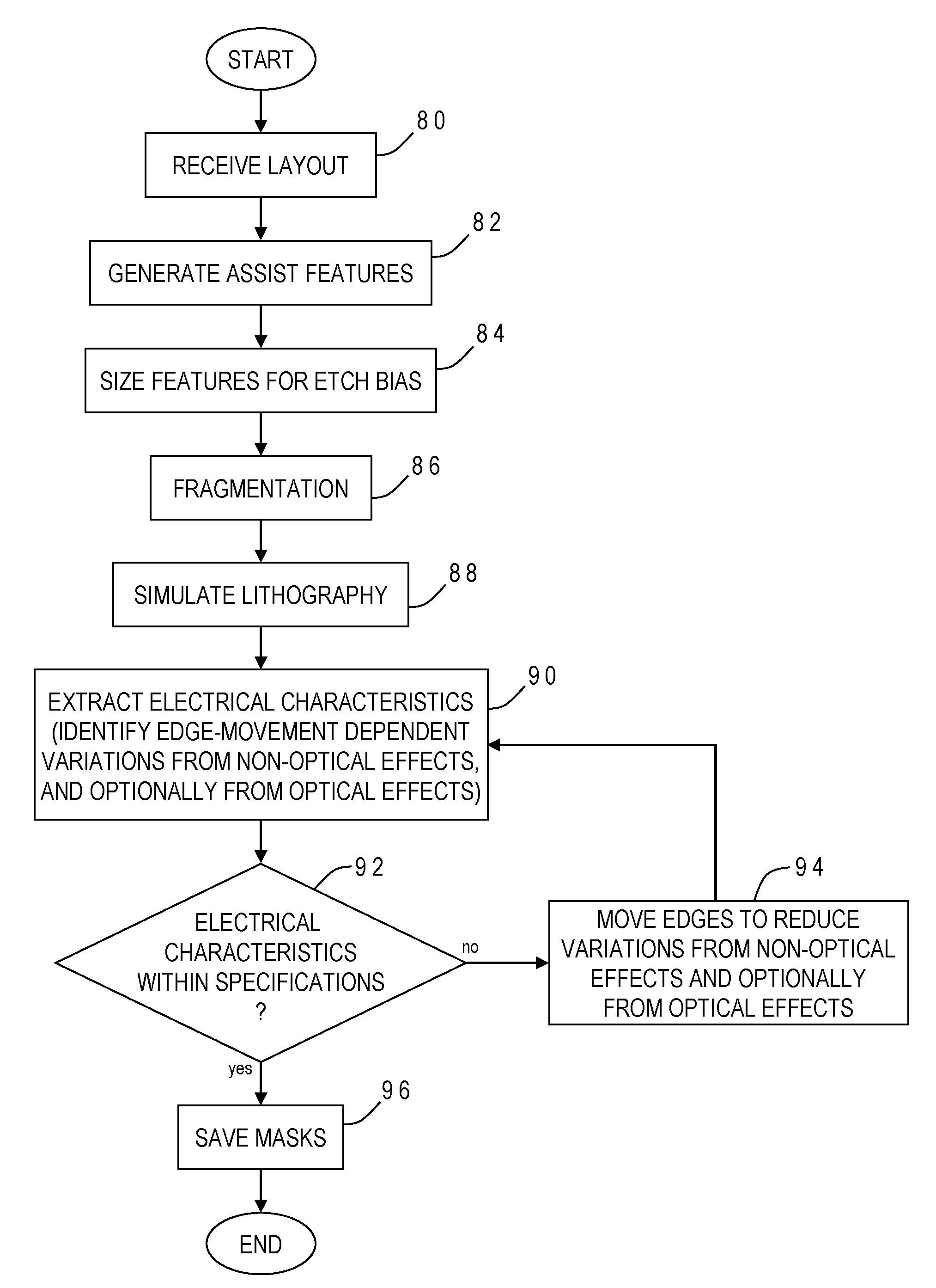
[0014]The foregoing objects are achieved in a method of improving performance of an integrated circuit design, by receiving a physical layout of the integrated circuit design, converting the physical layout into a mask design having a shape feature with a contour, simulating a photolithographic construction of a portion of an integrated circuit chip based on the mask design, extracting an electrical characteristic from the simulated integrated circuit chip which is affected by at least one fabrication variation arising from non-optical effects, establishing that the extracted electrical characteristic is not within a design specification, and responsively modifying the contour to reduce the fabrication variation by moving one or more edge sections of the contour until the electrical characteristic is within the design specification. The fabrication variation may arise from non-optical effects such as stress, well proximity, rapid thermal anneal, or spacer thickness.

Problems solved by technology

An IC may include a very large number of cells and require complicated connections between the cells.
Chip performance and yield are increasingly limited by systematic and random variations introduced during wafer processing.
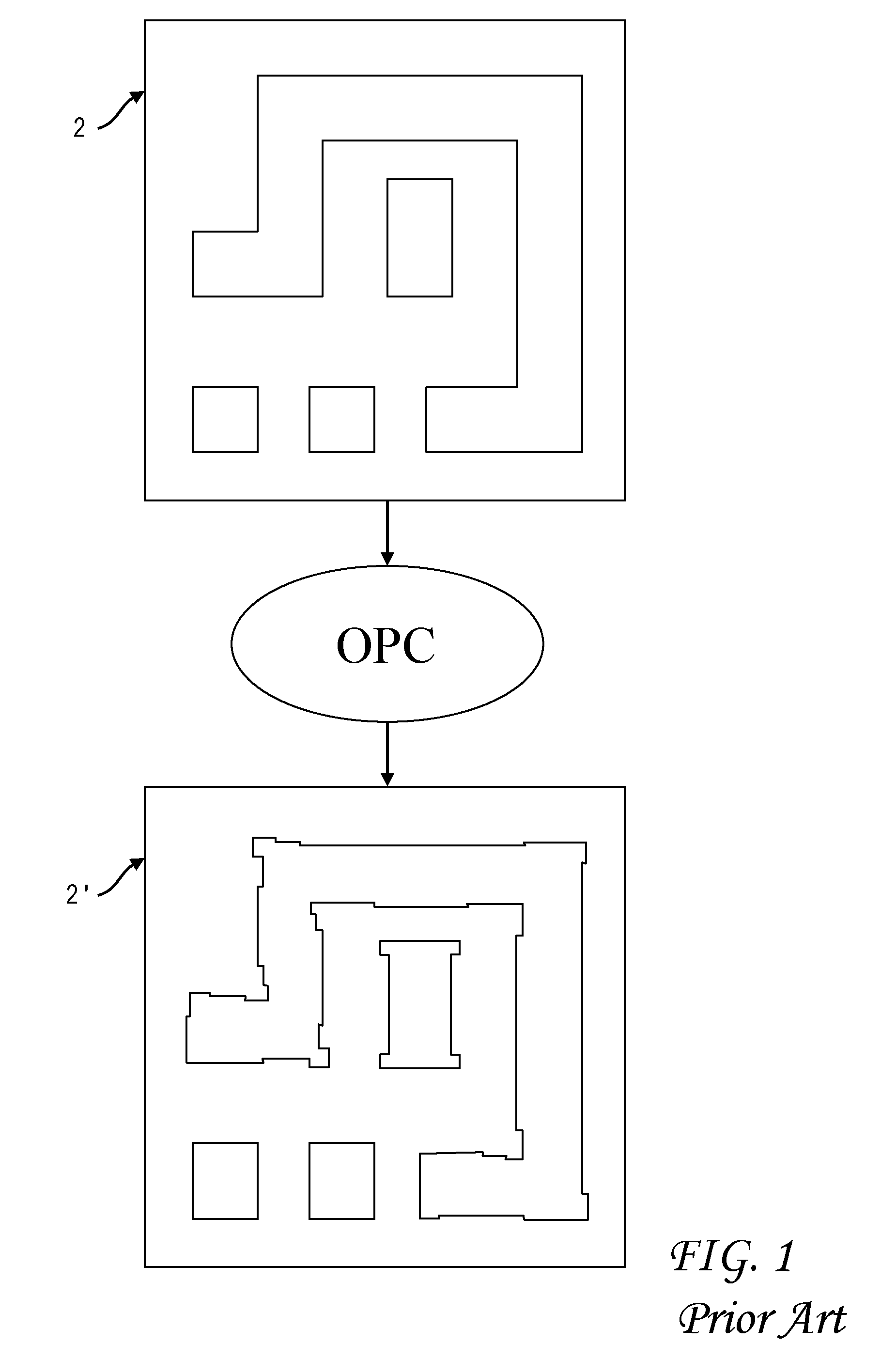
Optical effects such as pitch-dependent line width variations, flare, corner rounding and line-end shortening all affect electrical properties of devices forming the integrated circuit, and can easily render a chip defective.
While OPC is useful in reducing optical variations, it has its limitations.
Minimizing edge placement errors does not necessarily guarantee the best electrical behavior, and non-ideal electrical behavior will adversely affect cell leakage and circuit timing.
There is no standard technique to compensate for non-optical effects.
While circuit simulators like SPICE are straightforward and fairly quick to run, if the simulation is not set up properly the results can be inaccurate.
Also, while SPICE models are able to capture layout-dependent variations such as stress and well proximity, other non-optical effects such as spacer thickness and RTA cannot be captured in the device models due to lack of knowledge of the cell neighborhood, and hence these effects cannot be accounted for at design time.
However, gate length biasing may produce inaccurate results since it is performed with coarse discrete increments.

Method used


Image

  • Electrically-driven optical proximity correction to compensate for non-optical effects
  • Electrically-driven optical proximity correction to compensate for non-optical effects
  • Electrically-driven optical proximity correction to compensate for non-optical effects

Examples


Embodiment Construction

)

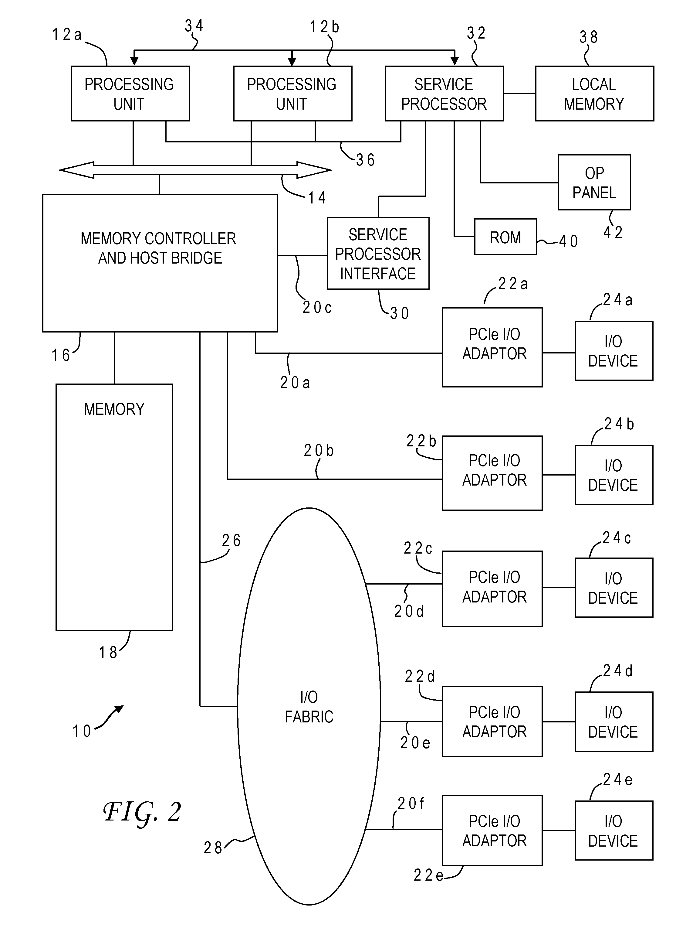
[0025]With reference now to the figures, and in particular with reference to FIG. 2, there is depicted one embodiment 10 of a computer system in which the present invention may be implemented to carry out the design of an integrated circuit. Computer system 10 is a symmetric multiprocessor (SMP) system having a plurality of processors 12a, 12b connected to a system bus 14. System bus 14 is further connected to a combined memory controller / host bridge (MC / HB) 16 which provides an interface to system memory 18. System memory 18 may be a local memory device or alternatively may include a plurality of distributed memory devices, preferably dynamic random-access memory (DRAM). There may be additional structures in the memory hierarchy which are not depicted, such as on-board (L1) and second-level (L2) or third-level (L3) caches.

[0026]MC / HB 16 also has an interface to peripheral component interconnect (PCI) Express links 20a, 20b, 20c. Each PCI Express (PCIe)link 20a, 20b is connected to...


PUM


Abstract

A contour of a mask design for an integrated circuit is modified to compensate for systematic variations arising from non-optical effects such as stress, well proximity, rapid thermal anneal, or spacer thickness. Electrical characteristics of a simulated integrated circuit chip fabricated using the mask design are extracted and compared to design specifications, and one or more edges of the contour are adjusted to reduce the systematic variation until the electrical characteristic is within specification. The particular electrical characteristic preferably depends on which layer is to be fabricated from the mask: on-current for a polysilicon; resistance for contact; resistance and capacitance for metal; current for active; and resistance for vias. For systematic threshold voltage variation, the contour is adjusted to match a gate length which corresponds to an on-current value according to pre-calculated curves for contour current and gate length at a nominal threshold voltage of the chip.

Description

BACKGROUND OF THE INVENTION[0001]1. Field of the Invention[0002]The present invention generally relates to the design and fabrication of integrated circuit chips from silicon wafers, and more particularly to a method of correcting deficiencies in an integrated circuit design which is manufactured using circuit pattern masks and photolithography.[0003]2. Description of the Related Art[0004]Integrated circuits are used for a wide variety of electronic applications, from simple devices such as wristwatches, to the most complex computer systems. A microelectronic integrated circuit (IC) chip can generally be thought of as a collection of logic cells with electrical interconnections between the cells, formed on a semiconductor substrate (e.g., silicon). An IC may include a very large number of cells and require complicated connections between the cells. A cell is a group of one or more circuit elements such as transistors, capacitors, resistors, inductors, and other basic circuit element...

Claims


Application Information

Patent Timeline
Patent Type & Authority Applications(United States)
IPC IPC(8): G06F17/50
CPCG03F1/144G06F2217/10G06F17/5081G03F1/36G06F30/398G06F2111/08G03F7/70441
Inventor AGARWAL, KANAK B.BANERJEE, SHAYAKELAKKUMANAN, PRAVEENLIEBMANN, LARS W.
Owner SIEMENS PROD LIFECYCLE MANAGEMENT SOFTWARE INC
Learn More