Dye sensitized photoelectric conversion device and manufacturing method thereof, electronic equipment, and semiconductor electrode and manufacturing method thereof

a sensitized photoelectric and manufacturing method technology, applied in the direction of sustainable manufacturing/processing, final product manufacturing, transportation and packaging, etc., can solve the problems of low productivity, disadvantage in view of cost, and large installation burden, and achieve the effect of reducing the efficiency of photoelectric conversion and remarkably lowering the quantum yield

Inactive Publication Date: 2010-05-13
SONY CORP
View PDF37 Cites 23 Cited by
  • Summary
  • Abstract
  • Description
  • Claims
  • Application Information

AI Technical Summary

Benefits of technology

[0024]As described above, since a sufficient light absorption cannot be obtained with one kind of dye, it may be considered to use a plurality kinds of dyes with absorption wavelength characteristics different from each other in admixture as a sensitizing dye. However, when the plurality kinds of dyes are used being mixed on the semiconductor layer 103, the photoelectric conversion efficiency is actually lowered in most cases. This is because the ratio for obtaining a current from absorbed photons, that is, a quantum yield is remarkably lowered, for example, by electron transfer between dyes as already described.
[0045]There is no particular restriction on the grain size of the fine semiconductor particles but it is preferably from 1 to 200 nm, particularly preferably, from 5 to 100 nm as an average grain size of primary particles. Further, it is also possible to mix the fine semiconductor particles of the average grain size described above with fine semiconductor particles of an average grain size larger than the average grain size described above, thereby scattering incident light by the fine semiconductor particles of the larger average grain size to improve the quantum yield. In this case, the average grain size of the fine semiconductor particles mixed additionally is preferably from 20 to 500 nm.
[0048]For the counter electrode any material can be used so long as this is the conductive substance and even an insulative substance can also be used so long as a conductive layer is disposed on the side facing the semiconductor electrode. However, it is preferred to use an electrochemically stable material for the counter electrode material and, specifically, use of platinum, gold, carbon, a conductive polymer, etc. is desired. Further, with an aim of improving the effect of the redox catalyst, it is preferred that the side facing the semiconductor electrode is in a fine structure to increase the surface area. For example, it is desirably in a platinum black state in a case of platinum and in a porous state in a case of carbon. The state of platinum black can be formed by an anodizing method of platinum, a chloroplatinic acid treatment, or the like and carbon in the porous state can be formed by a method, for example, of sintering fine carbon particles or baking an organic polymer. Further, by wiring a metal of high redox catalytic effect such as platinum on a transparent conductive substrate, or applying a chloroplatinic acid treatment to the surface, it can be used as a transparent counter electrode.
[0049]As the electrolyte, a combination of iodine (I2) and a metal iodide or an organic iodide or a combination of bromine (Br2) and a metal bromide or an organic bromide, as well as a metal complex such as ferrocyanate salt / ferricyanate salt or ferrocene / ferricinium ion, sulfur compounds such as sodium polysulfide, alkylthiol / alkyldisulfide, viologen dyes, hydroquinone / quinine, etc. can be used. Li, Na, K, Mg, Ca, Cs, etc. are preferred as the cations of the metal compounds and quaternary ammonium compounds such as tetraalkyl ammoniums, pyridiniums, imidazoliums, etc. are preferred as the cation of the organic compounds but they are not restricted to them, or two or more of them may be used in admixture. Among them, the electrolyte including a combination of I2 and LiI, NaI or a quaternary ammonium compound such as imidazolinium iodide is preferred. The concentration of the electrolyte salt to the solvent is, preferably, from 0.05 to 10 M and, more preferably, from 0.2 to 3 M. The concentration for I2 or Br2 is, preferably, from 0.0005 to 1 M and, more preferably, from 0.001 to 0.5 M. Further, with an aim of improving the open voltage and short circuit current, various additives such as 4-tert-butylpyridine or benzimidazoliums may also be added.
[0051]With an aim of decreasing the liquid leakage from the photoelectric conversion device and evaporation of the electrolyte, a gelling agent, polymer, crosslinking monomer, etc. may be dissolved into the electrolyte composition and can be used as the gel-like electrolyte. For the ratio for the gel matrix and the electrolyte composition, while the ionic conductivity is higher, the mechanical strength is lowered as the electrolyte composition is increased. On the contrary, while the mechanical strength is higher, the ionic conductivity is lowered when the electrolyte composition is excessively decreased. Then, the electrolyte composition is preferably from 50 to 99 wt % and, more preferably, from 80 to 97 wt % for the gel-like electrolyte. Further, an entirely solid type photoelectric conversion device can also be materialized by dissolving the electrolyte and the plasticizer in a polymer, evaporating and removing the plasticizer.

Problems solved by technology

However, in the crystalline silicon solar cells, while the photoelectronic conversion efficiency representing the performance of converting light (solar) energy into electric energy is higher compared with that of the amorphous silicon solar cells, since they require much energy and time for crystal growth, the productivity is low and they are disadvantageous in view of the cost.
Further, while the amorphous silicon solar cells have higher productivity compared with that of the crystallize silicon solar cells, they also require a vacuum process for the production in the same manner as in the crystalline silicon solar cells and the burden in term of installation is still large.
However, the photoelectric conversion efficiency of most of the solar cells is as low as about 1%, and they have not yet been put to practical use.
Considering that the open voltage is higher in the dye sensitized photoelectric conversion device than in the crystalline silicon solar cell, it is considered that the low photoelectric conversion efficiency of the dye sensitized solar cell is caused by the fact that the photo-current obtained is extremely smaller compared with the crystalline silicon solar cell and this is mainly attributable to that the light absorption rate of the dye 107 is insufficient.
That is, it is considered that since a dye capable of efficiently absorbing all the lights of various wavelengths contained in solar light is not present, the light absorption rate is insufficient in a dye sensitized solar cell using one kind of dye.

Method used


Image

  • Dye sensitized photoelectric conversion device and manufacturing method thereof, electronic equipment, and semiconductor electrode and manufacturing method thereof
  • Dye sensitized photoelectric conversion device and manufacturing method thereof, electronic equipment, and semiconductor electrode and manufacturing method thereof
  • Dye sensitized photoelectric conversion device and manufacturing method thereof, electronic equipment, and semiconductor electrode and manufacturing method thereof

Examples


example

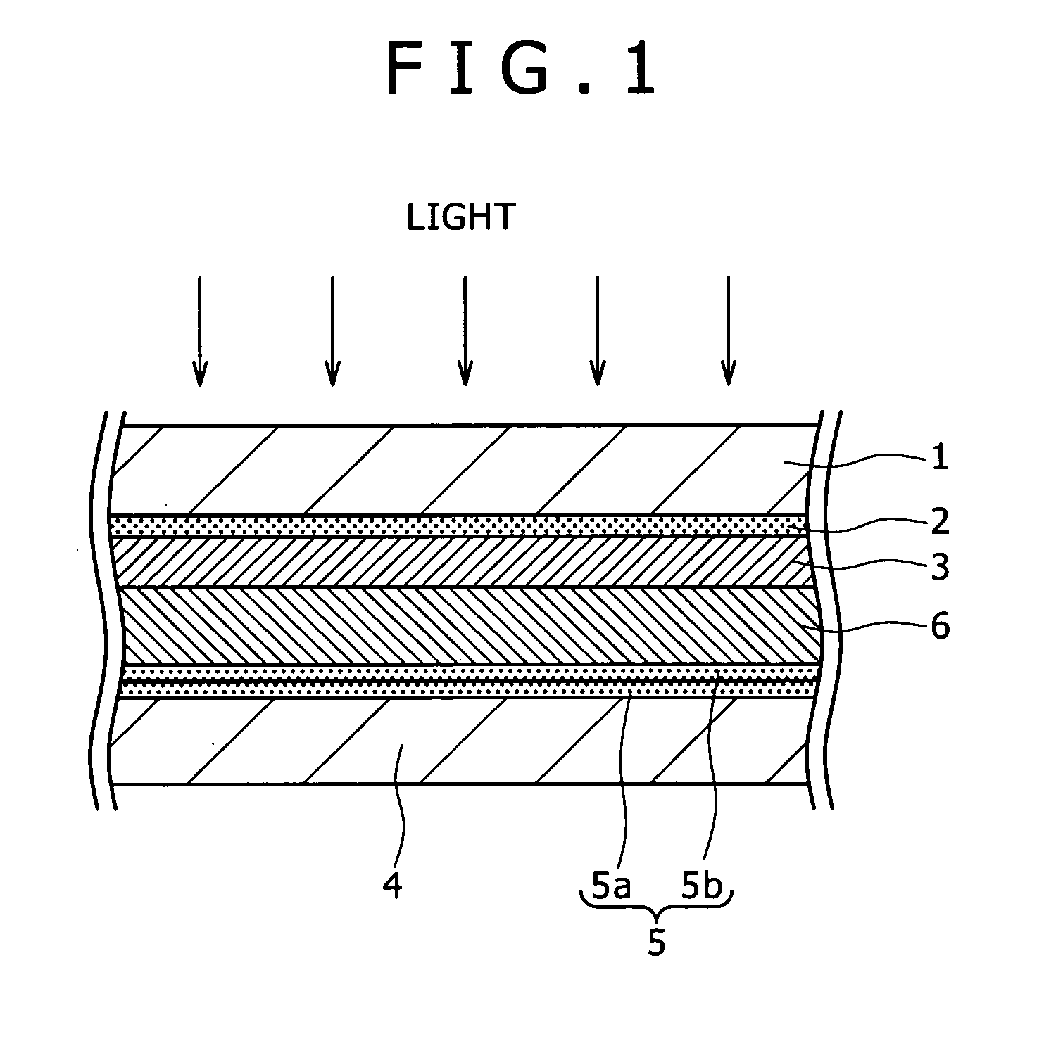
[0092]Fine TiO2 particles were used as the fine semiconductor particles. A paste in which fine TiO2 particles were dispersed was prepared with reference to Hironori Arakawa, “Recent Advances in Research and Development for Dye-Sensitized Solar Cells” (CMC) p. 45-47 (2001) as described below. 125 mL of titanium isopropoxide was dropped slowly into 750 mL of an aqueous solution of 0.1M nitric acid under stirring at a room temperature. After the completion of the dropping, the solution was transferred to a thermostable bath at 80° C., and stirred for 8 hours to obtain a clouded semi-transparent sol solution. After that, the sol solution was allowed to cool to a room temperature, and filtered through a glass filter, and it was measured up to 700 mL. The obtained sol solution was transferred to an autoclave and, after hydrothermic treatment at 220° C. for 12 hours, applied with a dispersing treatment by conducting a supersonic treatment for 1 hour. Next, the solution was concentrated by ...


PUM


Abstract

In a dye sensitized photoelectric conversion device having an electrolyte layer (6) between a semiconductor electrode (3) including, for example, fine semiconductor particles to which a sensitizing dye is adsorbed and a counter electrode (5), two kinds of dyes are used as the dye, and the two kinds of dyes are adsorbed onto the surface of the semiconductor electrode (3) at the sites different from each other. The fine semiconductor particles include, for example, TiO2. Tris(isothiocyanate)-ruthenium(II)-2,2′:6′,2″-terpyridine-4,4′,4″-tricarboxylic acid and 2-cyano-3-[4-[4-(2,2-diphenylethenyl)phenyl]-1,2,3,3a,4,8b-hexahydrocyclopent[b]indol-7-yl]-2-propenoic acid are used, for example, as the two kinds of dyes. Thereby, a dye sensitized photoelectric conversion device such as a dye sensitized solar cell capable of obtaining higher light absorption rate and photoelectric conversion efficiency than in a case of using one kind of dye at high purity, as well as a manufacturing method thereof are provided.

Description

TECHNICAL FIELD[0001]The present invention relates to a dye sensitized photoelectric conversion device and a manufacturing method thereof, an electronic equipment, and a semiconductor electrode and a manufacturing method thereof, which are suitable to application, for example, in a dye sensitized solar cell using a semiconductor electrode including fine semiconductor particles to which a sensitizing dye is adsorbed.BACKGROUND ART[0002]Since a solar cell as a photoelectric conversion device for converting solar light into electric energy uses the solar light as an energy source, it gives extremely less effect on global environments and a further popularization has been expected.[0003]While various materials have been studied for solar cells, a number of those using silicon have been marketed and they are generally classified into crystalline silicon type solar cells using single crystal or polycrystal silicon, and noncrystalline (amorphous) silicon type solar cells. Heretofore, singl...

Claims


Application Information

Patent Timeline
IPC IPC(8): H01L31/00H01L31/18H01L31/0232H01L31/0224
CPCH01G9/2031H01G9/2059H01G9/2063Y02E10/542Y02T10/7022Y02P70/521Y02T10/70Y02P70/50H01L31/04
Inventor YONEYA, REIKOMOROOKA, MASAHIROSUZUKI, YUSUKE
Owner SONY CORP
Why Eureka
Try Eureka