Solar cell module and method for manufacturing solar cell module
a solar cell module and solar cell technology, applied in the field of solar cell modules, can solve the problems etc., and achieve the effects of reducing the photoelectric conversion efficiency of the solar cell module, reducing the photogenerated carrier generated in each of the solar cell elements, and deteriorating the transparent conductive layer
- Summary
- Abstract
- Description
- Claims
- Application Information
AI Technical Summary
Benefits of technology
Problems solved by technology
Method used
Image

Examples
first embodiment
(Schematic Configuration of Solar Cell Module)
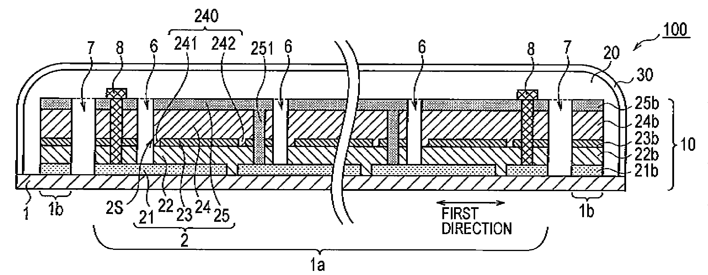
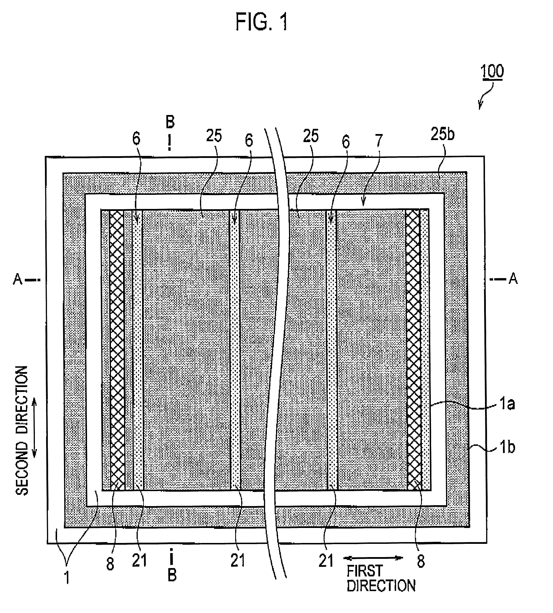
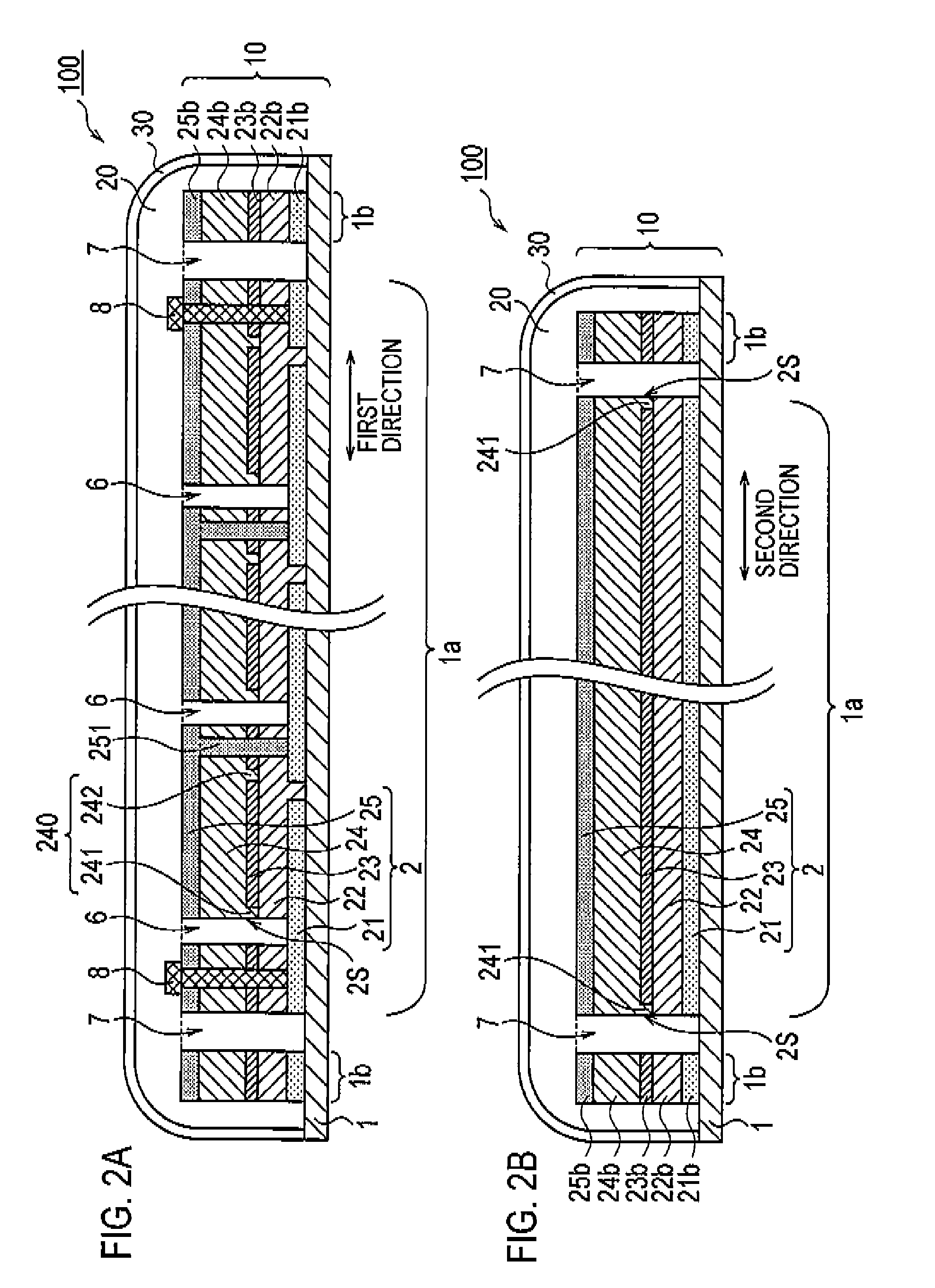
[0031]With reference to FIG. 1, a schematic configuration of a solar cell module 100 according to a first embodiment of the present invention will be described below. FIG. 1 is a top view of the solar cell module 100 according to the first embodiment of the present invention. Note that in FIG. 1, a filler 20 and a protector 30 are removed therefrom. Moreover, FIGS. 2A and 2B are cross-sectional views of the solar cell module 100. Note that FIG. 2A is a cross-sectional view along the line A-A in FIG. 1 and FIG. 28 is a cross-sectional view along the line B-B in FIG. 1, As shown in FIGS. 1, 2A and 2B, the solar cell module 100 includes a solar cell 10, the filler 20 and the protector 30.
[0032]The solar cell 10 includes a power generation region 1a and a non-power generation region 1b surrounding the power generation region 1a and being spaced apart therefrom. A configuration of the solar cell will be described later.
[0033]The filler 20 is ...
second embodiment
[0070]A second embodiment of the present invention will be described below. Note that the following description will be mainly given of differences between the first embodiment described above and the second embodiment.
(Configuration of Solar Cell)
[0071]FIG. 8 is a cross-sectional view of a solar cell module 100 according to the second embodiment of the present invention. As shown in FIG. 8, a second semiconductor layer 24 has a first extension part 241 and a second extension part 242.
[0072]In the second embodiment, the second extension part 242 is extended toward the first electrode layer 21 and is in contact with the first electrode layer 21. In other words, the second extension part 242 is formed between the first semiconductor layer 22 and a connection part 251.
(Advantageous Effects)
[0073]The second semiconductor layer 24 according to the second embodiment of the present invention is extended toward the first electrode layer 21 and is in contact with the first electrode layer 21...
third embodiment
[0074]A third embodiment of the present invention will be described below. Note that the following description will be mainly given of differences between the first embodiment described above and the third embodiment.
(Configuration of Solar Cell)
[0075]FIG. 9 is a cross-sectional view of a solar cell module 100 according to the third embodiment of the present invention. As shown in FIG. 9, the solar cell element 2 has a conductive part 9a and an insulating part 9b.
[0076]The conductive part 9a in one solar cell element 2 is in contact with a first electrode layer 21 in another solar cell element 2 adjacent to the one solar cell element 2. The one and another as described above. Specifically, the conductive part 9a has the same function as that of the connection part 251 according to the first embodiment of the present invention. As the conductive part 9a, a metal material having conductivity or the like can be used. However, the conductive part 9a is not limited thereto.
[0077]The ins...
PUM
 Abstract
Description
Claims
Application Information
 - R&D
- Intellectual Property
- Life Sciences
- Materials
- Tech Scout
- Unparalleled Data Quality
- Higher Quality Content
- 60% Fewer Hallucinations
Browse by: Latest US Patents, China's latest patents, Technical Efficacy Thesaurus, Application Domain, Technology Topic, Popular Technical Reports.
© 2025 PatSnap. All rights reserved.Legal|Privacy policy|Modern Slavery Act Transparency Statement|Sitemap|About US| Contact US: help@patsnap.com