Semiconductor light emitting device, its manufacturing method, semiconductor device and its manufacturing method

a technology of semiconductors and light emitting devices, applied in the direction of lasers, nanoinformatics, semiconductor lasers, etc., can solve the problems of large stress generation in the active layer, deterioration deterioration of the active layer, etc., to achieve good crystalline quality, improve the effect of thickness and reduce the stress

Inactive Publication Date: 2008-03-04
SONY CORP
View PDF8 Cites 6 Cited by
  • Summary
  • Abstract
  • Description
  • Claims
  • Application Information

AI Technical Summary

Benefits of technology

[0012]For manufacturing a semiconductor laser using nitride III-V compound semiconductors, in general, for the purpose of preventing deterioration of its active layer by elimination of In or preventing overflow of electrons injected into the active layer in the process of growing a p-type optical guide layer or a p-type clad layer on the active layer of InGaN, or the like, at a high growth temperature around 1000° C., the active layer is first grown, then an approximately 20 nm thick cap layer of p-type AlGaN having Al composition as high as approximately 0.2 is next grown at the same temperature as the active layer, and a p-type optical guide layer ad a p-type clad layer are grown at a raised growth temperature. However, according to the knowledge of the Inventor, although this structure certainly prevents deterioration of the active layer by elimination of In, a large difference in lattice constant between the cap layer and the active layer causes generation of a large stress in the active layer in contact with the cap layer, and this invites deterioration of the active layer. Furthermore, although Mg is typically used as the p-type dopant of p-type layers, diffusion of Mg from the p-type layers into the active layer also causes deterioration of the active layer.
[0014]After further researches, the Inventor has also found that, in case a nitride III-V compound semiconductor containing In, such as InGaN, is grown while the flow rate of In source material is maintained in the same level after growth of the uppermost barrier layer of the active layer having a multi-quantum well structure, quantity of In can be adequately controlled at the growth temperature. Thus, by using it upon growing such a nitride III-V compound semiconductor containing In, such as InGaN, since the growth temperature can be raised during the growth and the cap layer can therefore be grown at a raised growth temperature to improve the crystalline quality, the cap layer can be reduced in thickness or can be even omitted in the ultimate case exclusively from the viewpoint of preventing elimination of In from the active layer.
[0015]On the other hand, as to the position where the cap layer should be located in the laser structure, namely between the active layer and the p-type clad layer, there still remains room for improvement. Under the situation, the Inventor made efforts to optimize the position of the cap layer while taking account of assuring design choice, and has found some optimum positions from the viewpoints of improving the crystalline quality of the optical guide layer and improving symmetry of intensity distribution of light in far-field images. Furthermore, the Inventor has found various advantages when the aforementioned nitride III-V compound semiconductor layer containing In and Ga, such as InGaN, is provided in contact with the active layer in addition to optimizing the position of the cap layer.
[0044]The active layer made of the first nitride III-V compound semiconductor, or the layer made of the first nitride III-V compound semiconductor, typically has a multi-quantum well structure including well layers and barrier layers. In this case, composition of In in the intermediate layer is equal to or smaller than the In composition of the barrier layers. Various kinds of distribution of the In composition are acceptable. If the intermediate layer is grown while the growth temperature is gradually raised, the intermediate layer can be formed to gradually decrease in composition of In toward its portion remotest from the active layer or the layer made of the first nitride III-V compound semiconductor. Quantity of In contained in the intermediate layer is typically equal to or less than 5×1019 cm−3. Thickness of the intermediate layer is determined such that the intermediate layer can effectively prevent deterioration of the active layer or the layer made of the first nitride III-V compound semiconductor, in accordance with its composition selected. Typically, the thickness is controlled to be equal to or more than 8 nm, and preferably to be equal to or more than 10 nm.
[0237]According to the invention summarized above, since the intermediate layer made of the second nitride III-V compound semiconductor containing In and Ga and different from the first nitride III-V compound semiconductor is provided in contact with the active layer or the layer made of the first nitride III-V compound semiconductor, the intermediate layer largely alleviates the stress produced in the active layer or the layer made of the first nitride III-V compound semiconductor, or effectively prevents Mg used as the p-type dopant from diffusion into the active layer or the layer made of the first nitride III-V compound semiconductor.
[0238]Additionally, by optimizing the position of the cap layer, the optical guide layer or the first optical guide layer can be grown in a good crystalline quality as compared with a structure locating the cap layer adjacent to the active layer via the intermediate layer, for example, or the optical guide layer or the first optical guide layer can be optimized in thickness.

Problems solved by technology

However, according to the knowledge of the Inventor, although this structure certainly prevents deterioration of the active layer by elimination of In, a large difference in lattice constant between the cap layer and the active layer causes generation of a large stress in the active layer in contact with the cap layer, and this invites deterioration of the active layer.
Furthermore, although Mg is typically used as the p-type dopant of p-type layers, diffusion of Mg from the p-type layers into the active layer also causes deterioration of the active layer.

Method used


Image

  • Semiconductor light emitting device, its manufacturing method, semiconductor device and its manufacturing method
  • Semiconductor light emitting device, its manufacturing method, semiconductor device and its manufacturing method
  • Semiconductor light emitting device, its manufacturing method, semiconductor device and its manufacturing method

Examples


first embodiment

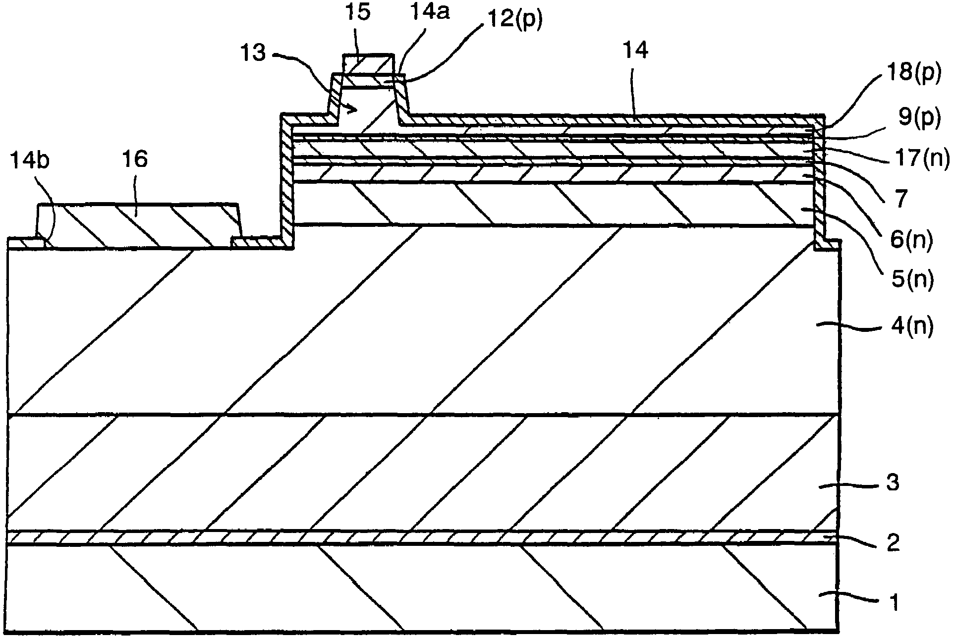
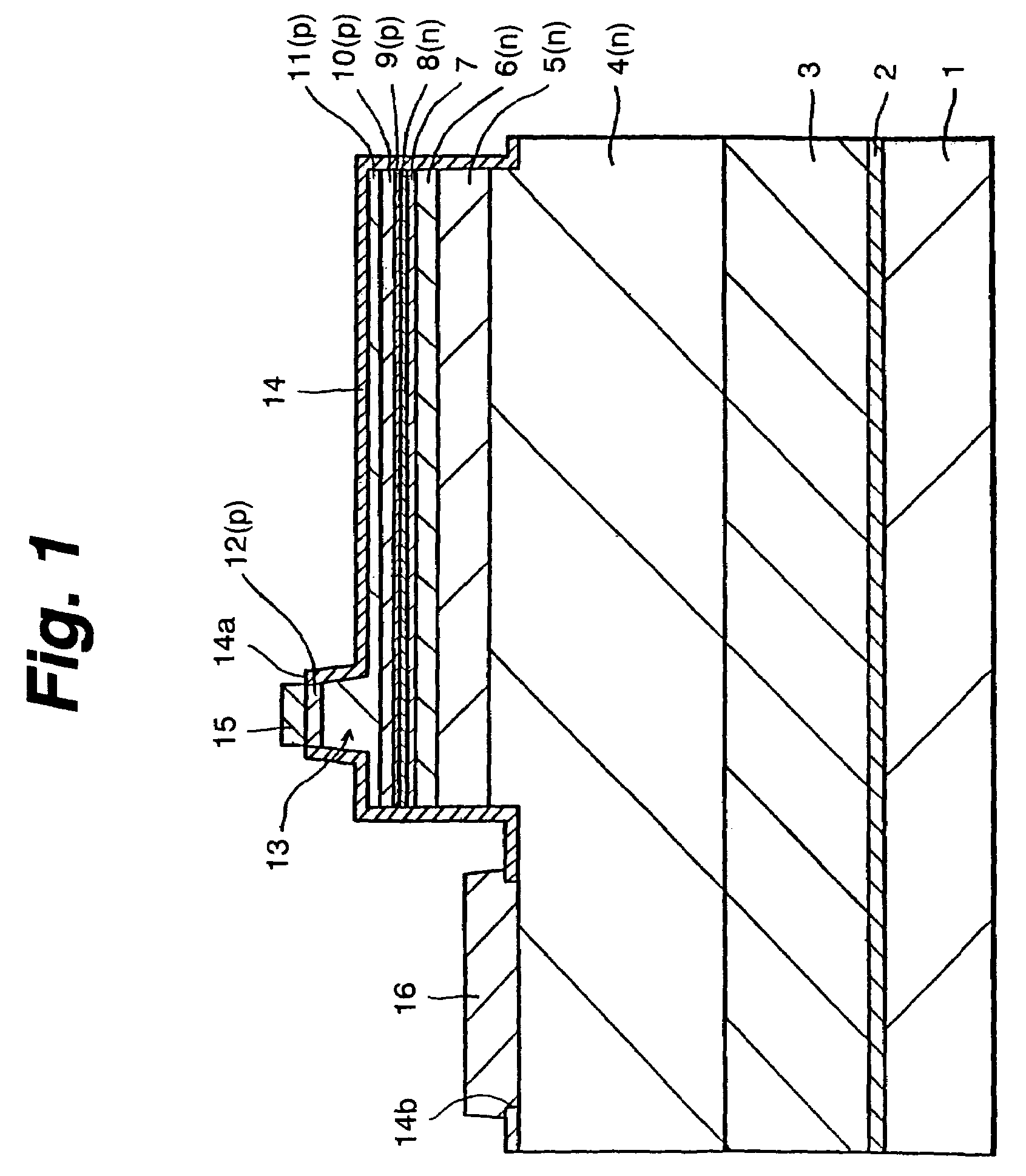
[0257]FIG. 1 shows a GaN compound semiconductor laser according to the invention. This GaN compound semiconductor laser has a ridge structure and a SCH (separate confinement heterostructure) structure.

[0258]As shown in FIG. 1, the GaN compound semiconductor laser according to the first embodiment includes an undoped GaN layer 3 grown by lateral crystal growth technique such as ELO: n-type GaN contact layer 4; n-type AlGaN clad layer 5; n-type GaN optical guide layer 6; active layer 7 having an undoped InxGa1-xN / InyGa1-yN multiquantum well structure, for example; n-type undoped InGaN deterioration preventing layer 8; p-type AlGaN cap layer 9; p-type GaN optical guide layer 10; p-type AlGaN clad layer 11; and p-type GaN contact layer 12 that are sequentially overlaid on a c-plane sapphire substrate 1 via an undoped GaN buffer layer 2 grown at a low temperature.

[0259]The undoped GaN buffer layer 2 is 30 nm thick, for example. The undoped GaN layer 3 is 0.5 μm thick, for example. The n-...

second embodiment

[0281]Next explained is a GaN compound semiconductor laser according to the invention. FIG. 3 is an energy band diagram of this GaN compound semiconductor laser.

[0282]In the GaN compound semiconductor laser according to the second embodiment, Indium composition in the undoped InGaN deterioration preventing layer is uniform throughout the entire thickness thereof, and the indium composition is adjusted to a value smaller than the Indium composition y of the barrier layers in the active layer 7, namely 0.02, for example. In the other respects, its structure is identical to that of the GaN compound semiconductor laser according to the first embodiment. So, its explanation is omitted here.

[0283]This GaN compound semiconductor laser can be manufactured by the same method as that of the GaN compound semiconductor laser according to the first embodiment except that the undoped InGaN deterioration preventing layer 8 is grown under a constant growth temperature.

[0284]The second embodiment al...

third embodiment

[0285]Next explained is a GaN compound semiconductor laser according to the invention. FIG. 4 is an energy band diagram of this GaN compound semiconductor laser.

[0286]In the GaN compound semiconductor laser according to the third embodiment, Indium composition of the undoped InGaN deterioration preventing layer is uniform throughout the entire thickness thereof, and the indium composition is adjusted to the same value as the Indium composition y of the barrier layers in the active layer 7. Thickness of the undoped InGaN deterioration preventing layer 8 is adjusted such that the sum of its own thickness and the thickness of one of the barrier layers of the active layer 7 nearest thereto is at least 15 nm, preferably not thinner than 17 nm, more preferably not thinner than 20 nm, or still more preferably not thinner than 25 nm. In the other respects, its structure is identical to that of the GaN compound semiconductor laser according to the first embodiment. So, its explanation is omi...


PUM

PropertyMeasurementUnit
thicknessaaaaaaaaaa
thicknessaaaaaaaaaa
thicknessaaaaaaaaaa

Abstract

A semiconductor light emitting device made of nitride III-V compound semiconductors includes an active layer made of a first nitride III-V compound semiconductor containing In and Ga, such as InGaN; an intermediate layer made of a second nitride III-V compound semiconductor containing In and Ga and different from the first nitride III-V compound semiconductor, such as InGaN; and a cap layer made of a third nitride III-V compound semiconductor containing Al and Ga, such as p-type AlGaN, which are deposited in sequential contact.

Description

RELATED APPLICATION [0001]This application is a continuation of PCT Application No. PCT / JP01 / 11536 filed Dec. 27, 2001, which claims priority to Japanese applications Nos. P2000-401998 filed Dec. 28, 2000, and P2001-271947 filed Sep. 7, 2001, all of which are incorporated herein by reference to the extent permitted by law.BACKGROUND OF THE INVENTION [0002]This invention relates to a semiconductor light emitting device and a manufacturing method thereof, as well as a semiconductor device and a manufacturing method thereof, especially suitable for applications to semiconductor lasers, light emitting diodes or electron transporting devices made by using nitride III-V compound semiconductors.[0003]Semiconductor lasers made of AlGaInN or other nitride III-V compound semiconductors are under active researches and developments as semiconductor lasers capable of emitting light from the blue region to the ultraviolet region required for enhancing the density of optical discs.[0004]Japanese P...

Claims


Application Information

Patent Timeline
Patent Type & Authority Patents(United States)
IPC IPC(8): H01L27/15H01L33/00H01L21/205B82Y10/00B82Y20/00B82Y40/00H01S5/20H01S5/22H01S5/323H01S5/343
CPCB82Y20/00H01L33/0075H01L33/06H01L33/32H01S5/34333H01L33/04H01S5/0425H01S5/2004H01S5/2013H01S5/3201H01S2301/173H01S2304/12H01S5/04257
Inventor GOTO, OSAMUASANO, TAKEHARUSUZUKI, YASUHIKOTAKEYA, MOTONOBUSHIBUYA, KATSUYOSHIMIZUNO, TAKASHITOJO, TSUYOSHIUCHIDA, SHIROIKEDA, MASAO
Owner SONY CORP
Why Eureka
Try Eureka