Light-Emitting Component

a technology of light-emitting components and components, which is applied in the direction of organic semiconductor devices, electroluminescent light sources, thermoelectric devices, etc., can solve the problems of not more than two different polymer layers, the sequence of the structure of a given material system can be changed with a great amount of difficulty, and disadvantages, etc., to achieve good structure capability of light-emitting devices, improve the flexibility of structure, and improve the injection of charge carriers

Active Publication Date: 2010-03-18
NOVALED GMBH
View PDF99 Cites 3 Cited by
  • Summary
  • Abstract
  • Description
  • Claims
  • Application Information

AI Technical Summary

Benefits of technology

[0022]The task of the invention is to provide for a light-emitting device with increased flexibility with regard to the structure and improved injection of charge carriers from the electric contacts in the light-emitting layer stacks. In addition, a good structuring capability of the light-emitting device is to be maintained in this case.
[0027]By means of the combination of the polymer layer from the polymer material and the low-molecular layer with the vacuum-deposited small molecules of an organic material in the light-emitting device a higher flexibility for the light-emitting layer stack is obtained, wherein with the formation of the polymer layer an easier structuring capability of the device for producing pixel areas, which emit light in various colours, is obtained without the necessity of having to use shadow masks as normally used for light-emitting organic devices which are formed on the basis of small molecules of organic materials.
[0028]There is the advantage furthermore that the material for the electrode contacts is freely selectable. Possible losses during the injection of charge carriers are minimised or even avoided totally. Stable light-emitting devices with a long life service have been created. The otherwise conventional co-evaporation of organic materials is not necessary.
[0062]A purposeful embodiment of the invention can envisage that the arrangement of layers with the substrate is transparent.
[0065]The inclusion of the low-molecular layers from one or several organic materials serves to avoid a restriction of the modification of the polymer layers resulting from the existence of normally only two disjoint solvents for the depositing of the polymer materials, and in this way it increases the variation options of the layer structure of the device. During the manufacture of the light-emitting device, the donor and / or the acceptor molecules for the low-molecular layer(s) can be produced at first in the vacuum from a precursor by evaporating an organic basic material acting as the precursor, and this basic material forms the donor / acceptor molecules during the evaporation process.

Problems solved by technology

The disadvantage of the known PLED structures is, among other things, the fact that not more than two different polymer layers can be deposited in a suitable manner because the solvents of the polymer materials must be selected in such a way that they do not influence each other, meaning, that they do not attack the material of the substructure.
In addition, the sequence of the structure for a given material system can be changed with a great amount of difficulty only.
This is particularly disadvantageous for the integration of the PLED structure on active matrix display substrates with n-channel transistors as a contact element.
The use of transparent top contacts is also difficult because these (i) have an unfavourable work function for the electron injection (work function is too great) and (ii) are usually manufactured by means of a sputtering process.
However, this process destroys organic materials.
In this ease also, however, the electron injection from the cathode contact is a problem.
A further disadvantage of the conventional PLED structure is the fact that an efficient electron injection can be obtained with only very unstable contact materials such as barium or calcium.
These materials, however, are attacked by oxygen and water.
Moreover, it is very difficult to use one and the same electrode (cathode) for all emitter materials of the three basic emission colours red, green and blue because this involves considerable performance losses with one of the three colours.
An optimised cathode contact for the blue-emitting polymer material has disadvantages for the red-emitting polymer material, and vice versa.
The disadvantage of such devices is that a lateral structuring of the OLED-structure for the configuration of differently coloured pixels in a display is normally performed with shadow masks.
This process has limitations with regard to the smallest obtainable pixel sizes which are less than approximately 50 μm.
Shadow masking in a manufacturing process involves a relatively considerable work effort.
The inkjet process as used for depositing polymer materials is either not useable or only useable with limitations for small molecules during the formation of low molecular layers due to the non-solubility of the organic materials of the small molecules.
LITI (“Laser Induced Thermal Imaging”) is an alternative process which, on its part, has limitations particularly with the selection of the process-compatible materials.
However, with this arrangement the injection of charge carriers, namely electrons from the cathode contact into the low-molecular electron transport layer, is problematic.

Method used


Image

  • Light-Emitting Component
  • Light-Emitting Component

Examples


example 1

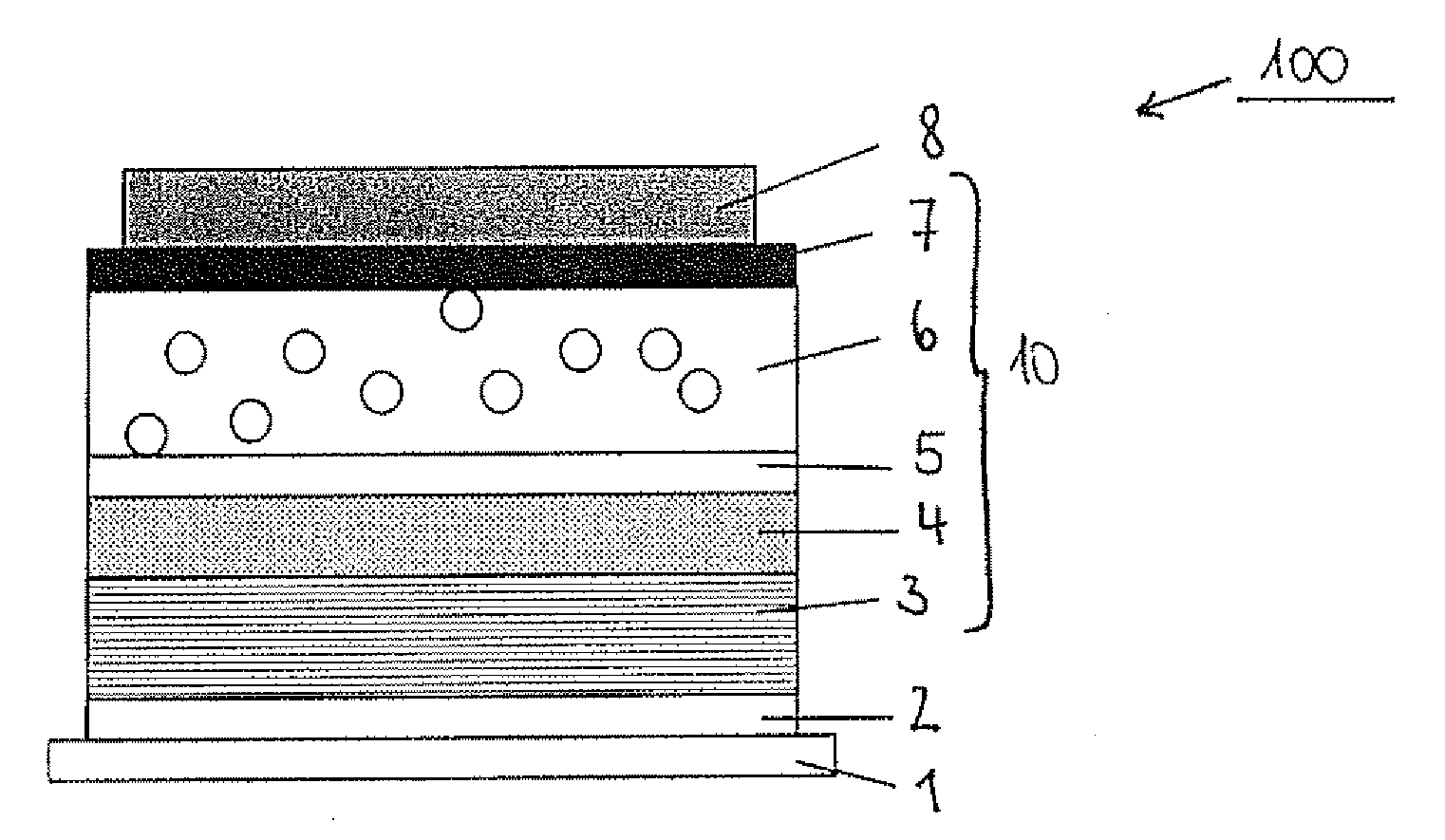
[0080]According to an example 1 the light-emitting device has the following structure, which comprises a low-molecular organic injection layer from donor molecules of an organic material:[0081]1.1 transparent substrate (glass)[0082]1.2 anode contact (indium tin oxide ITO; 90 nm thick)[0083]1.3 polymer hole injection layer, (PEDOT:PSS (Baytron-P of H.C. Starck, Germany); 80 nm thick (spin-coated from watery dispersion)[0084]1.4 polymer hole transporting emission layer (MEH-PPV; 70 nm thick (spin-coated from toluene solution)[0085]1.7 low-molecular donor molecule layer (W2(Xpp)4; 2 nm thick)[0086]1.8 cathode contact (reflecting; Al)

example 2

[0087]According to an example 2 the light-emitting device has the following structure, which comprises a low-molecular organic injection layer from donor molecules of an organic material:[0088]2.1 transparent substrate (glass)[0089]2.2 anode contact (indium tin oxide ITO; 90 nm thick)[0090]2.3 polymer hole injection layer, (PEDOT:PSS (Baytron-P of H.C. Starck, Germany); 80 nm thick (spin-coated from watery dispersion)[0091]2.4 polymer hole transporting emission layer (MEH-PPV; 60 nm thick (spin-coated from toluene solution)[0092]2.6 n-doped low-molecular electron transport layer (from Alq3 doped with W2(Xpp)4, mass doping concentration 20% (corresponds to a molar doping concentration of approx. 10%); 20 nm thick)[0093]2.7 low-molecular donor molecule layer (W2(Xpp)4; 2 nm thick)[0094]2.8 cathode contact (reflecting; Al)

[0095]By means of the insertion of the n-doped electron transport layer 2.6, the optic cavity of the hybrid device can be adapted without incurring losses with regard...

example 3

[0096]According to an example 3 the light-emitting device has the following structure, which comprises a low-molecular organic injection layer from donor molecules of an organic material:[0097]3.1 transparent substrate (glass)[0098]3.2 anode contact (indium tin oxide ITO; 90 nm thick)[0099]3.3 polymer hole injection layer, (PEDOT:PSS (Baytron-P of H.C. Starck, Germany); 80 nm thick (spin-coated from watery dispersion)[0100]3.4 polymer hole transporting emission layer (MEH-PPV; 60 nm thick (spin-coated from toluene solution)[0101]3.6 low-molecular electron transport layer (from Alq3; 20 nm thick)[0102]3.7 low-molecular donor molecule layer (W2(Xpp)4; 2 nm thick)[0103]3.8 cathode contact (reflecting; Al)

[0104]In contrast to example 2, this device has a non-doped low-molecular electron transport layer. Compared with example 2, there were slight losses with regard to the measured operating voltage as a result. However, a mixed evaporation process can be dispensed with.


PUM

PropertyMeasurementUnit
reduction potentialaaaaaaaaaa

Abstract

The invention relates to a light-emitting device, in particular a light-emitting diode, with an arrangement of layers on a substrate, wherein the arrangement of layers has an anode contact and a cathode contact which are in electrical contact with a light-emitting layer stack arranged between the anode contact and the cathode contact which, on its part, comprises a polymer layer consisting of a polymer material and a low-molecular layer of vacuum-deposited small molecules of an organic material, and wherein the small molecules of the low-molecular layer are formed as donor molecules with an oxidation potential versus Fc / Fc+ (ferrocene / ferrocenium redox couple) of maximum approx. −1.5 V, if the low-molecular layer is arranged adjacent to the cathode contact, and as acceptor molecules with a reduction potential versus Fc / Fc+ (ferrocene / ferrocenium redox couple) of minimum approx. −0.3 V if the low-molecular layer is arranged adjacent to the anode contact.

Description

[0001]The invention relates to a light-emitting device, in particular a light-emitting diode, with an arrangement of layers on a substrate wherein the arrangement of layers comprises an anode contact and a cathode contact as well as a light-emitting layer stack, arranged between the anode contact and the cathode contact, having a polymer layer consisting of a polymer material and a low-molecular layer with small molecules of an organic material deposited in a vacuum.BACKGROUND OF THE INVENTION[0002]Since the demonstration of low working voltages [compare Tang et al.: Appl. Phys. Lett. 51 (12), 913 (1987)], organic light-emitting diodes have become promising candidates for the realisation of large-surface displays and other applications such as illuminating elements. They comprise an arrangement of thin layers of organic materials. Either, the layers are preferably vapour-deposited in a vacuum in the form of molecules. Low-molecular layers are formed in this way. An organic light-emi...

Claims


Application Information

Patent Timeline
Patent Type & Authority Applications(United States)
IPC IPC(8): H01L51/52
CPCH01L51/0037H01L51/0038H01L51/0051H01L51/0077H01L51/0079H01L2251/554H01L51/0085H01L51/5052H01L51/5088H01L51/5092H01L51/5096H01L51/0084H10K85/1135H10K85/114H10K85/611H10K85/30H10K85/321H10K85/341H10K85/342H10K50/155H10K50/165H10K50/171H10K50/18H10K50/17H10K2101/50H05B33/10
Inventor BIRNSTOCK, JANBLOCHWITZ-NIMOTH, JAN
Owner NOVALED GMBH
Why Eureka
Try Eureka