One-time programmable read only memory

Inactive Publication Date: 2010-03-11
KIM JUHAN
View PDF6 Cites 25 Cited by
  • Summary
  • Abstract
  • Description
  • Claims
  • Application Information

AI Technical Summary

Benefits of technology

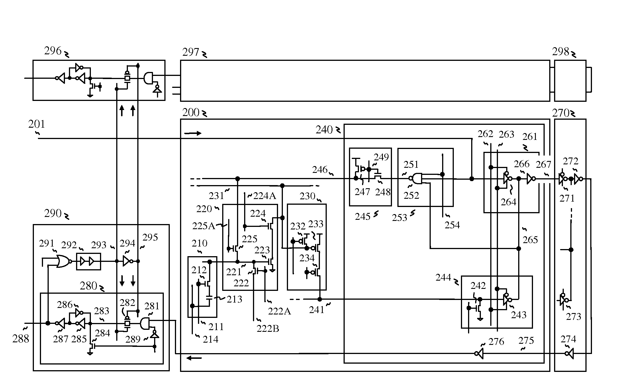
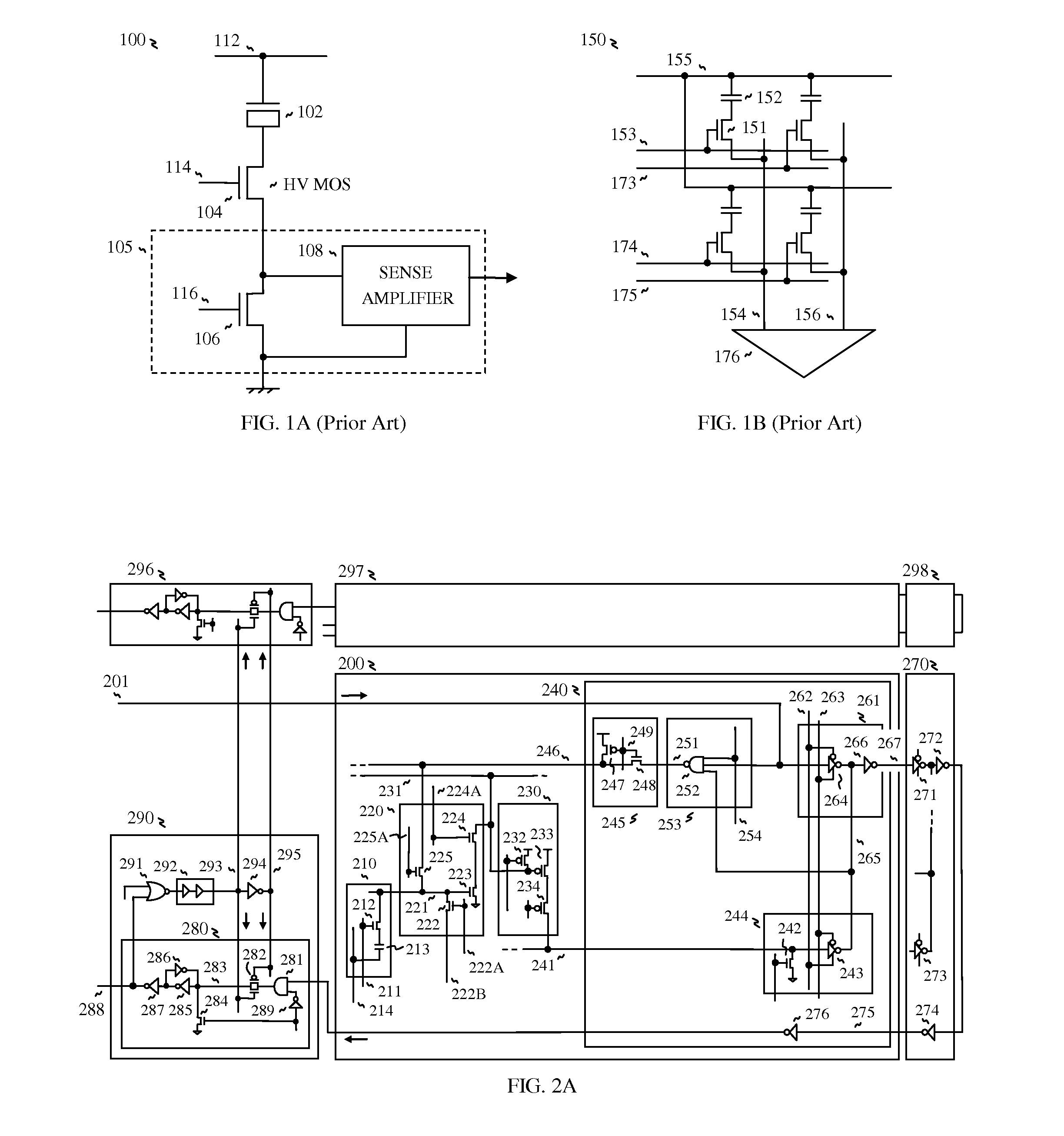
[0009]For realizing high speed read operation for the OTP memory, bit line is multi-divided, which reduces parasitic capacitance, so that the divided bit line is quickly charged when reading and multi-stage sense amps are used for connecting divided bit line, wherein the multi-stage sense amps are composed of dynamic circuits for realizing fast access and eliminating penetration current when reading. More specifically, the multi-stage sense amps include a first dynamic circuit serving as a local sense amp, a second dynamic circuit serving as a segment sense amp, and a first tri-state inverter serving as an amplify circuit of a global sense amp, while a second tri-state inverter is used for bypassing an output from a previous memory block, which configures a data transfer circuit. The dynamic circuits are also useful to reduce operating voltage for realizing low power consumption, because the dynamic circuits are turned on around threshold voltage of MOS transistor for detecting whether the amplify circuit is turned on or not by a selected memory cell. With multi-stage sense amp, fast read operation is realized because each sense amp drives a lightly loaded and divided bit line, such that the memory cell drives the lightly loaded local bit line, the local sense amp drives a segment bit line for transferring a read output to the segment sense amp, the segment sense amp drives a global bit line for transferring the read output to the global sense amp, and the global sense amp drives a very lightly loaded common node of the data transfer circuit for transferring the read output to an output latch circuit.
[0011]And, amplifying transistors of the sense amps are composed of relatively long channel transistors, in order to reduce turn-off current, which reduces power consumption.
[0013]Furthermore, configuring the memory is more flexible, such that number of sense amps can be determined by the target speed. For example, high speed application needs more segmented array with more sense amps, while high density application needs more memory cells with reduced number of sense amps, thus cell efficiency is increased.
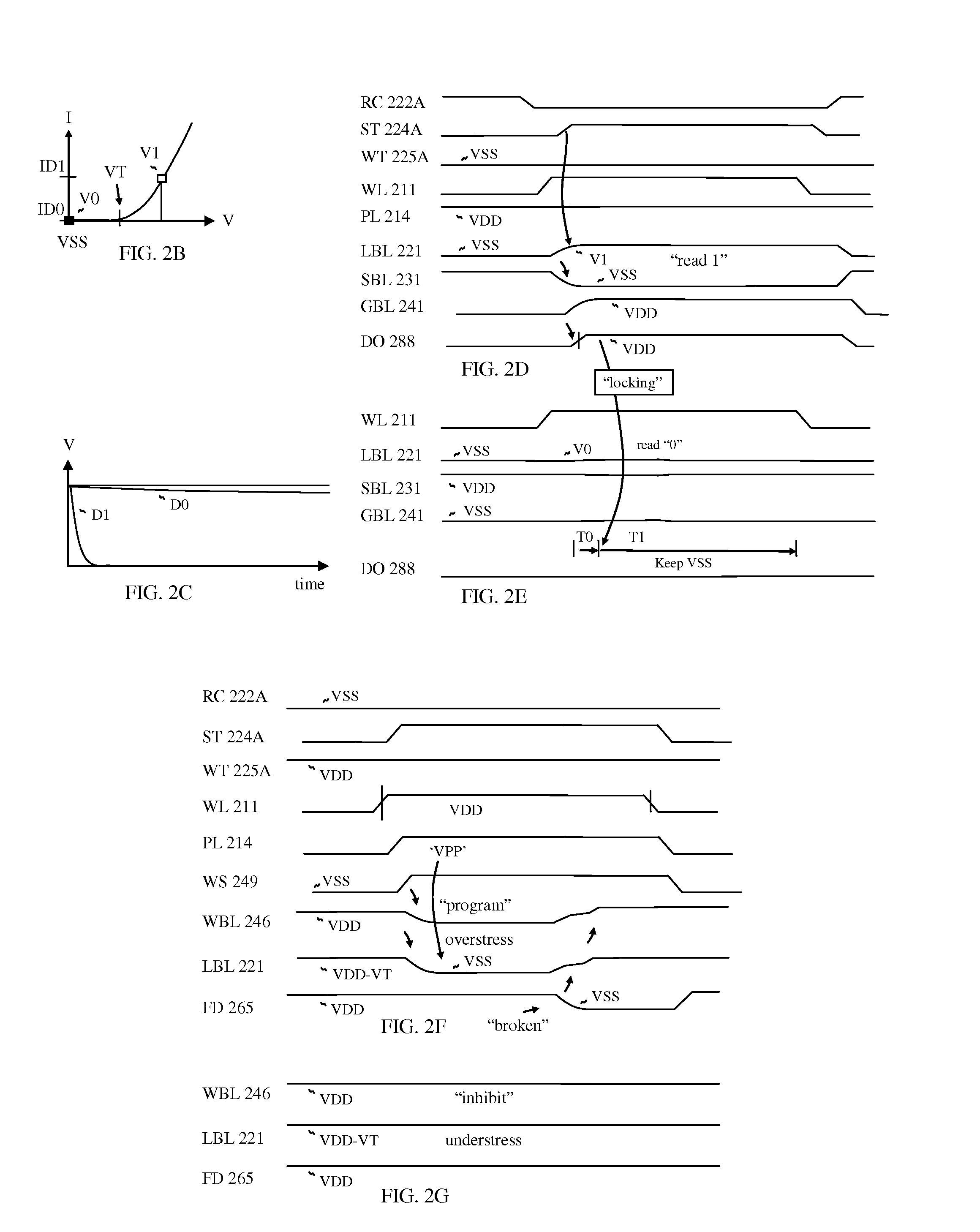
[0016]More specifically, a reference signal is generated by one of fast changing data with high gain from reference cells, which signal serves as a reference signal to generate a locking signal or a read duration control signal in order to reject latching another data which is slowly changed with low gain, such that high voltage data is arrived first while low voltage data is arrived later, or low voltage data is arrived first while high voltage data is arrived later depending on configuration. The time domain sensing scheme effectively differentiates high voltage data and low voltage data with time delay control, while the conventional sensing scheme is current-domain or voltage-domain sensing scheme. In the convention memory, the selected memory cell discharges the local bit line, and the discharged voltage of the local bit line is compared by a comparator which determines an output at a time. There are many advantages to realize the time domain sensing scheme, so that the sensing time is easily controlled by a tunable delay circuit, which compensates cell-to-cell variation and wafer-to-wafer variation, such that there is a need for adding a delay time before locking the latch circuit with a statistical data for all the memory cells, such as mean time between fast data and slow data. Thereby the tunable delay circuit generates a delay time for optimum range. And the read output from the memory cell is transferred to the latch circuit through a returning read path, thus the access time is equal regardless of the location of the selected memory cell, which is advantageous to transfer the read output to the external pad at a time.
[0017]When programming the memory cell, the multi-stage sense amp serves as a current detector to cut off a current path after blown. In doing so, data pattern sensitivity is reduced when programming. Without the current detector circuit, maximum current flows when programming all “1” (blown) or no current flows when programming all “0” (not blown).
[0018]Furthermore, the memory cell can be reduced because the memory cell only drives a lightly loaded local bit line when reading, and also the current flow of the pass transistor can be reduced, which means that the memory cell can be miniaturized further. Moreover, the present invention realizes multi-stacked memory cell structure including thin film transistor because the memory cell only drives lightly loaded bit line even though thin film polysilicon transistor can flow lower current, around 10 times lower, for example.

Problems solved by technology

Such charge storage approaches, however, are not practicable with current and deep sub-micron technologies that feature very thin gate oxide because of the high gate leakage current that prevents a long retention time of the information.
However, the common plate line may cause data pattern sensitivity when programming all “1” (blown) or all “0” (not blown).
Hence, gate oxide of unselected memory cell may be destroyed during programming.
Furthermore, the local bit line 154 is heavily loaded with conventional sensing scheme which includes differential amplifier, so that charging time of the local bit line is slow, which is one of obstacles for achieving fast read operation.

Method used


Image

  • One-time programmable read only memory
  • One-time programmable read only memory
  • One-time programmable read only memory

Examples


Embodiment Construction

)

[0034]Reference is made in detail to the preferred embodiments of the invention. While the invention is described in conjunction with the preferred embodiments, the invention is not intended to be limited by these preferred embodiments. On the contrary, the invention is intended to cover alternatives, modifications and equivalents, which may be included within the spirit and scope of the invention as defined by the appended claims. Furthermore, in the following detailed description of the invention, numerous specific details are set forth in order to provide a thorough understanding of the invention. However, as is obvious to one ordinarily skilled in the art, the invention may be practiced without these specific details. In other instances, well-known methods, procedures, components, and circuits have not been described in detail so that aspects of the invention will not be obscured.

[0035]The present invention is directed to OTP (one time programmable) read only memory as shown in...


PUM


Abstract

For realizing high speed one time programmable memory, bit line is multi-divided for reducing capacitance, so that the bit line is quickly charged when reading and multi-stage sense amps are used for connecting divided bit line, wherein the multi-stage sense amps are composed of a first dynamic circuit serving as a local sense amp for reading the memory cell, a second dynamic circuit serving as a segment sense amp for reading the local sense amp, and a tri-state inverter serving as an amplify circuit of a global sense amp for reading the segment sense amp. When reading data, a voltage difference in the bit line is converted to a time difference for differentiating high data (programmed) and low data (unprogrammed) by the multi-stage sense amps. And buffered data path is connected to the global sense amp for realizing fast data transfer. Additionally, alternative circuits and memory cell structures are described.

Description

FIELD OF THE INVENTION[0001]The present invention relates to a semiconductor memory device, and more particularly, to OTP (One-Time Programmable) read only memory.BACKGROUND OF THE INVENTION[0002]OTP (One-Time Programmable) read only memory is used in integrated circuits for a variety of applications including nonvolatile memory applications. They may be used as a single memory cell, or in arrays of memory cells to provide unique chip identifications and to set operating parameters such as clock multipliers and voltage levels for devices such as microcontrollers and microprocessors, and also high-density memory applications for various applications. They may also be used to configure, customize, and repair a chip after testing, in order to repair a controller's cache memory array. One-time programmable memories are typically implemented using charge storage, fuse, or anti-fuse approaches. Charge storage approaches have typically involved defining a bit value based on charge stored o...

Claims


Application Information

Patent Timeline
IPC IPC(8): G11C17/04G11C7/00
CPCG11C7/06G11C7/18G11C2207/002G11C17/18G11C17/16
Inventor KIM, JUHAN
Owner KIM JUHAN
Why Eureka
Try Eureka