
Polymer pattern and metal film pattern, metal pattern, plastic mold using thereof, and method of the forming the same

a technology of metal film and polymer, applied in the field of polymer patterns, can solve the problems of many problems in cost and process stability, reducing the yield and uniformity of products, and unable to meet the diverse demands of three-dimensional structures, etc., and achieves the effects of high reliability, easy preparation, and improved cost competitiveness and easiness of processes

Inactive Publication Date: 2010-02-25
KOREA ADVANCED INST OF SCI & TECH
View PDF27 Cites 3 Cited by
  • Summary
  • Abstract
  • Description
  • Claims
  • Application Information

AI Technical Summary

Benefits of technology

[0067]As described above, the present invention has the effect capable of forming three-dimensional polymer patterns having various shapes using modifications of the means and methods used in the prior lithography process.
[0068]Also, the use of the polymer patterns according to the present invention allows the formation of positive photosensitive polymer patterns having an obtuse slope to the substrate. This can eliminate a need for the use a negative photosensitive polymer which is generally used in a lift-off process and the like. Thus, the cost competitiveness and easiness of processes can be improved.
[0069]Moreover, the metal film patterns formed using the inventive polymer patterns is very stable, can be easily prepared in various shapes, and can be used to form curved electrodes having high reliability. Such curved electrodes can be widely used in optical microshutters, microswitches and the like, and thus, can be regarded as having a very great commercial effect.
[0070]Also, the cantilever beams having a rounded cross-section can be formed with the metal film patterns formed using the inventive polymer patterns. This can solve the problem of stiction to the substrate, which has been a great problem in forming the cantilever beam according to the prior art.
[0071]Furthermore, the metal patterns formed using the inventive polymer patterns can be interconnected on devices having integrated circuits so as to improve the operating properties of the integrated circuits at high frequency.
[0072]Also, the plastic mold formed using the inventive polymer patterns can be prepared in a simpler process and lower material cost than those of the prior microscale fluidic channels. Also, this plastic mold can be used to make a microlens array whose optical properties can be controlled in a very simple manner.

Problems solved by technology

However, only with the prior polymer patterns or metal patterns having a rectangular shape, various demands for three-dimensional structures cannot be satisfied.
This is the main cause of remarkably reducing the yield and uniformity of products in the fabrication of cantilever beams.
However, these approaches have many problems in terms of cost and process stability.
However, in this case, it is very difficult to uniformly control the stress of the electrodes themselves, and thus, there is a problem in terms of process reproducibility.
Also, as the operating frequency increases, the parasitic capacitance between adjacent metal interconnections is gradually increased, thus causing deterioration in the performance of circuits.
However, in the case of forming the microlenses by this method, there are fatal problems in that the thermal and chemical stabilities of the lenses are insufficient and the process reproducibility is low (Z. D. Popovic, et. al., “Technique for the monolithic fabrication of microlens arrays”, Appl. Opt., Vol. 27, pp.
In addition, when the prior technology of thermally treating photosensitive polymers is used, there will be a problem in that it is very difficult to make a microlens array having a very high density (about 100%).
Also in the case of planar microlens arrays which are widely used for the communication between optical fibers or the biochips, there is a problem in that light is collected at a focal line, not at a focal point, due to the two-dimensional cylindrical shape of the lenses, thus reducing the light-collection efficiency of the lenses.

Method used


Image

  • Polymer pattern and metal film pattern, metal pattern, plastic mold using thereof, and method of the forming the same
  • Polymer pattern and metal film pattern, metal pattern, plastic mold using thereof, and method of the forming the same
  • Polymer pattern and metal film pattern, metal pattern, plastic mold using thereof, and method of the forming the same

Examples


embodiment 1

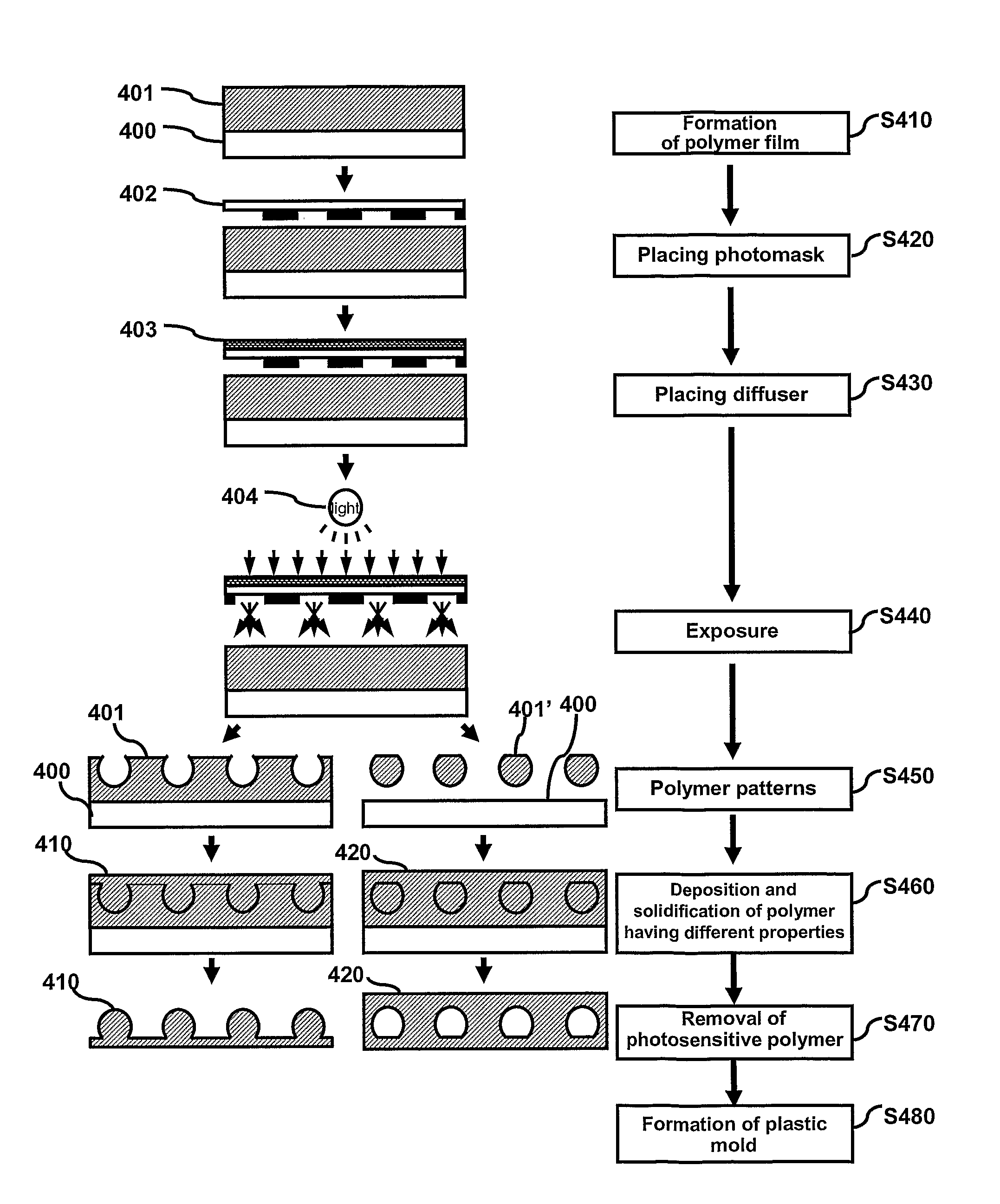
[0075]FIG. 3a is a perspective view of first polymer patterns formed according to the inventive lithography process, FIG. 3b is a cross-sectional view of the first polymer patterns formed according to the inventive lithography process, and FIG. 3c is a secondary electron microscopic photograph taken for a portion of the cross-section of the first polymer patterns.

[0076]Referring to FIGS. 3a to 3c, the first polymer patterns have the patterns 101a which are concave from the surface of the polymer film 101 deposited on the substrate 100 in a direction perpendicular to the substrate 100 and extend in a direction parallel to the substrate 100. The vertical cross-section of the concave patterns has at least one curved surface.

[0077]Namely, as shown in the drawings, the concave patterns 101a are so formed that they have a circular or oval shape, the top of which is cut in a straight line. These circular or oval patterns can vary in their shape or depth depending on the amount of UV applie...

embodiment 2

[0098]FIGS. 9a and 9b show the structure of first metal film patterns of a given shape according to the present invention, FIGS. 9c and 9d show the structure of second metal film patterns of a given shape according to the present invention, and FIGS. 9e and 9f show the structure of third metal film patterns of a given shape according to the present invention.

[0099]For reference, like reference numerals denote like elements throughout the drawings.

[0100]Referring to FIGS. 9a and 9b, the first metal film patterns 205 have pattern 205a which are concave in a direction perpendicular to the substrate 200 and extend in a direction parallel to the substrate 200. The vertical cross-section of the concave pattern 205a is open at its top and has at least one curved surface.

[0101]Depending on the formation position of the patterns, the first metal film patterns 205 are so formed that they are away from the substrate 200 so as to be suspended in space or are in contact with the substrate 200.

[0...

embodiment 3

[0121]FIGS. 12a and 12b show the structure of first metal patterns having a given shape according to the present invention, and FIGS. 12c and 12d show the structure of second metal patterns having a given shape according to the present invention.

[0122]As shown in FIGS. 12a and 12b, the first metal patterns 310 have concave patterns formed on the substrate 300 in a direction perpendicular to the substrate 300 and extending in a direction parallel to the substrate 300. The vertical cross-section of the concave patterns has at least one curved surface.

[0123]Namely, the concave patterns shown in FIGS. 12a and 12b have a rod shape with a circular or oval cross-section, the top of which is cut in a straight line. These circular or oval patterns can vary in their shape or depth depending on the amount of UV irradiated during the lithography process.

[0124]Depending on the formation position of the metal patterns, the first metal patterns 310 are away from the substrate 300 so as to be suspe...


PUM

PropertyMeasurementUnit
angleaaaaaaaaaa
shapeaaaaaaaaaa
densityaaaaaaaaaa

Abstract

The present invention relates to polymer patterns of various shapes formed using modifications of means and methods used in the prior lithography process, and the metal film patterns, metal patterns and plastic molds using the polymer patterns, as well as methods of forming these patterns and molds. The method of forming the polymer patterns comprises the steps of: (a) depositing a photosensitive polymer on the substrate to form a polymer film; (b) placing a photomask on the polymer film; and (c) irradiating the polymer film with a light moving in random direction through the photomask, so as to form at least one pattern which is concave from the surface of the polymer film in a direction perpendicular to the substrate and extends in a direction parallel to the substrate. The inventive polymer patterns have at least one pattern which is concave from the surface of the polymer film in a direction perpendicular to the substrate and extends in a direction parallel to the substrate. The vertical cross-section of the concave patterns has at least one curved surface.

Description

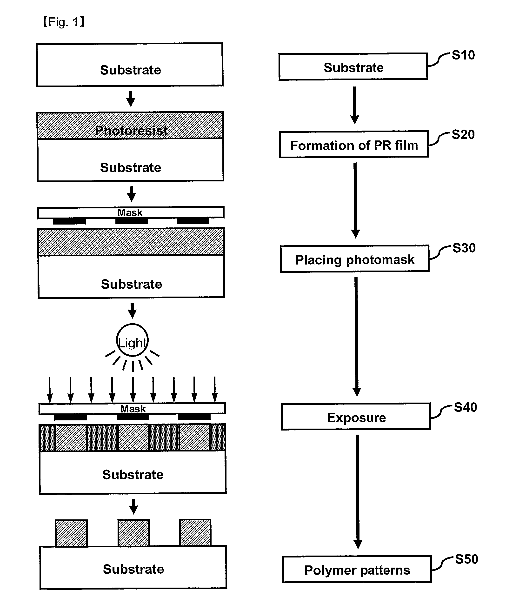
TECHNICAL FIELD [0001]The present invention relates to polymer patterns, and the metal film patterns, metal patterns and plastic molds using the polymer patterns, as well as methods of forming these patterns and molds. More particularly, the present invention relates to polymer patterns having a rounded shape which are formed using an incident light with random direction in a lithography process using a light source with a given wavelength, and to the metal film patterns, metal patterns and plastic molds formed using the same, as well as methods of forming these patterns and molds.BACKGROUND ART [0002]Generally, in order to form metal interconnections in semiconductor integrated circuits and the like, polymer patterns are first formed by a photolithography process including photoresist deposition, light exposure and development steps.[0003]FIG. 1 is a process flow diagram showing a method of forming positive photosensitive polymer patterns by the prior lithography process, and FIG. ...

Claims


Application Information

Patent Timeline
Patent Type & Authority Applications(United States)
IPC IPC(8): G02B27/12G03F7/20B32B3/00B29D11/00H01H57/00H05K1/00
CPCB81B2203/0118Y10T428/24479B81B2203/04B81C1/0015B81C1/00166G02B3/0012G02B3/0056G03F7/0005G03F7/201G03F7/2014H01L21/0272H01L21/0274H01L21/76885H01L23/5222B81B2203/019H01L2924/0002H01L2924/00
Inventor YOON, JUN-BOCHANG, SUNG-ILKIM, DAE-HYUNLEE, HYUNG SUKCHOI, JOON-YONGJANG, WEON-WILEE, KYUNGHO
Owner KOREA ADVANCED INST OF SCI & TECH
Learn More