Packaging structure and method for light-emitting diode

a technology of light-emitting diodes and packaging structures, applied in the direction of basic electric elements, electrical apparatus, semiconductor devices, etc., can solve the problems of increased cost and unpopular eutectic soldering methods, and achieve the effect of reducing the thermal resistance of packaging of light-emitting diodes

Inactive Publication Date: 2010-02-04
LO WEI HUNG
View PDF0 Cites 3 Cited by
  • Summary
  • Abstract
  • Description
  • Claims
  • Application Information

AI Technical Summary

Benefits of technology

[0008]The main objective of the present invention is to provide a packaging structure for light-emitting diode, which can greatly reduce the packaging thermal resistance of light-emitting diode.
[0009]A further objective of the present invention is to provide a packaging structure for light-emitting diode, in which silver paste is replaced with solder paste to reduce the time for heating as well as to reduce cost.

Problems solved by technology

However, the cost will be enhanced by adding eutectic soldering equipment.
The potential damage resulted from this frictional heating is not yet studied and thus the eutectic soldering approach is not popular.

Method used


Image

  • Packaging structure and method for light-emitting diode
  • Packaging structure and method for light-emitting diode
  • Packaging structure and method for light-emitting diode

Examples


Embodiment Construction

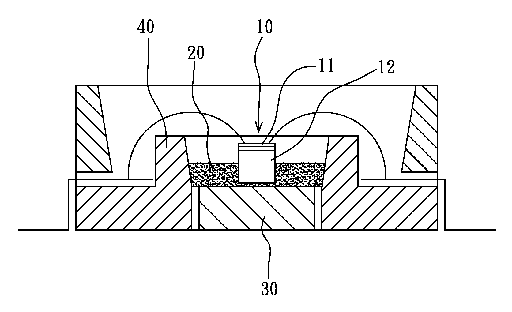
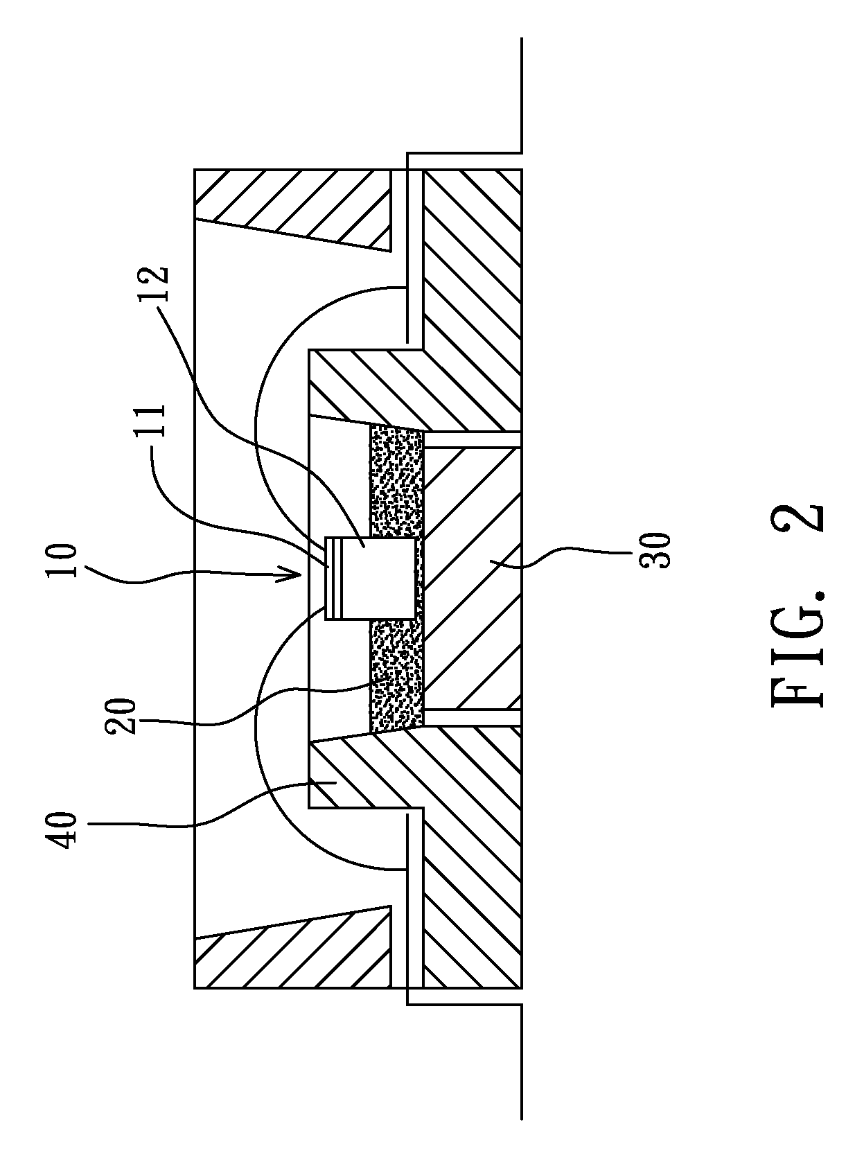
[0016]FIG. 2 illustrates a preferred embodiment of a packaging structure for light-emitting diode according to the present invention.

[0017]With reference to FIG. 2, a packaging structure for light-emitting diode according to the present invention comprises a grain 10, a solder paste layer 20, and a heat-conducting layer 30;

[0018]wherein the grain 10 is to provide electroluminescence, further comprising a luminescent layer 11 and a substrate 12, wherein the luminescent layer 11 is, for example but not limited to, an InGaN grain, which will be cited as an example for explanation in the present invention and which is not intended to limit the scope of the present invention; the substrate 12, which is, for example but not limited to, sapphire (Al2O3), copper alloy or monocrystal silicon, and is disposed under the luminescent layer 11 to connect the grain 10 with the solder paste layer 20. The thickness of the solder paste layer 20 may be 50˜90% of that of the grain 10, for example but n...


PUM

PropertyMeasurementUnit
thicknessaaaaaaaaaa
electroluminescenceaaaaaaaaaa
perimeteraaaaaaaaaa

Abstract

The present invention discloses a packaging structure for light-emitting diode, which comprises a grain to provide electroluminescence; a solder paste layer disposed on the bottom and perimeter of the grain to connect the grain with at least one support; and a heat-conducting layer disposed at the bottom of the grain to work as a heat-dissipating path for the grain, so that the aforementioned structure may significantly reduce the packaging thermal resistance of light-emitting diode. Further, the present invention also discloses a packaging method for light-emitting diode, which is capable of greatly reducing the packaging thermal resistance of light-emitting diode.

Description

FIELD OF THE INVENTION[0001]The present invention relates to a packaging structure and method for light-emitting diode, and in particular, to a packaging structure and method for light-emitting diode, which can significantly reduce the packaging thermal resistance of light-emitting diode.BACKGROUND OF THE INVENTION[0002]Light emitting diodes (abbreviated as LED) used at present are mostly high-power light-emitting diodes (power higher than 0.5 W) and efforts are being made to package high-power light-emitting diode with low thermal resistance (high heat dissipation) because the luminous efficacy of light-emitting diodes are closely related to temperature: luminous efficacy decreases as temperature increases. Therefore, the packaging of high-power light-emitting diode is developed toward fast heat dissipation, i.e. low thermal resistance.[0003]FIG. 1 illustrates the packaging structure of a conventional high-power light-emitting diode; as shown in the figure, the thermal resistance i...

Claims


Application Information

Patent Timeline
Patent Type & Authority Applications(United States)
IPC IPC(8): H01L33/00
CPCH01L33/64H01L2224/48091H01L2224/73265H01L2924/00014
Inventor NAUM, SOSHCHINLO, WEI-HUNGTSAI, CHI-RUEI
Owner LO WEI HUNG
Why Eureka
Try Eureka