
Wafer level chip scale packaging

a chip scale and wafer-level technology, applied in the field of low-cost process of wafer-level chip scale package, can solve the problems of increasing the performance limitation factor of conventional package, affecting the efficiency of the process, so as to achieve the effect of simple wafer-level csp process, more machines, and less material consumption

Active Publication Date: 2009-06-25
ALPHA & OMEGA SEMICON LTD
View PDF19 Cites 19 Cited by
  • Summary
  • Abstract
  • Description
  • Claims
  • Application Information

AI Technical Summary

Benefits of technology

[0017]As indicated at 206 in FIG. 2, conductive material 110 may cover the devices and fill the gaps between devices. The conductive material 110 may cover four side walls of the semiconductor chip 102. By way of example, conductive epoxy of cast conductive material 110, is then filled into the gaps 108 and over the top of drain electrode 107 and on the side of the semiconductor chips 102 as shown in FIG. 1C. By way of example, the conductive material 110 may be a Carbon material, such as nano carbon or carbon nanotubes. Alternatively the conductive material 110 may be a conductive adhesive, conductive epoxy, solder or the like. The conductive material 110 is disposed on the back side and side walls of the semiconductor chips 102 in such a way as to provide an electrical connection from the drain electrode 107 on the back side of the chip 102 to the front side of the chip. For the case in which the backside electrode 107 is comprised of the wafer substrate and not of metal, a cleaning step may optionally be introduced before the conductive material 110 is deposited in order to reduce any contaminants or oxidation which might be found on the wafer surface, thus ensuring better contact between the backside electrode 107 and conductive material 110. The cleaning solution can comprise of dilute HF, solvents, vapor-HF, etc.
[0018]As indicated at 206 in FIG. 2, the devices may be separated from each other by cutting through the conductive material 110 in the relatively wide gaps 108 between the devices. By way of example, the semiconductor chips 102 may be singulated by cutting through the cured conductive material between the chips with a narrow-bladed saw 112 to separate the wafer 100 into individual semiconductor devices 116 as shown in FIG. 1E. Preferably, the narrow-bladed saw 112 has a blade thickness that is less than the width of the gaps 108, e.g., if the gaps are about 80 to 100 microns wide, the thin-bladed saw 112 may have a blade thickness of about 20 to 30 microns. As the result a layer of conductive material coated over the back side surface and the side wall surfaces not only brings electrical connection from the back side electrode to the front surface but also protects the chip side surfaces from scratching, chipping, and other mechanical damage during final product electrical testing, packing, board level mounting and transportation.
[0020]Embodiments of the present invention allow true wafer-level processed chip scale packaging (CSP) of semiconductor devices with back to front connections with a minimum of added cost. A conventional CSP system may be used with relatively minor modifications, e.g., a thicker saw blade to provide gaps between adjacent die and apparatus for applying the conductive material over and between the die. Embodiments of the present invention open the door for the use of nano carbon coatings or carbon nanotubes (CNT) in drain connections.
[0022]Embodiments of the present invention allow for back to front electrical connections in a very simple wafer-level CSP process. This process does not require an assembly procedure for back-to-front drain connections. Prior art processes, by contrast, use assembly procedures that require more materials consumption and more machines.
[0023]In addition, the process described herein is very flexible at any die size without requiring tooling change for different sized die. Prior art techniques, by contrast, require either a new metal frame tool up or BGA mask change for different sized die, in addition to a machine conversion kit change, all of which can be very expensive. Further the difficulty of wafer warpage that occurs in many prior art wafer level chip-scale package (WLCSP) structures and processes due to thermal mismatch between the wafer and wafer back side coating material is no more a concern here because the above-described process saw the wafer into small chips before coating them with conductive material. This greatly reduces the potential thermal stress mismatch of wafer and coated material.

Problems solved by technology

Advances in semiconductor processing technology, however, have made parasitics (e.g., resistances, capacitances and inductances) associated with conventional packages more of a performance limiting factor.
In the case of conventional flip chip technology, among other shortcomings, heat dissipation is essentially governed by the die size and connection to the back side of the die is not easily facilitated (often requiring a bond wire connection).
These limitations (poor heat dissipation and resistive contact to back side) become quite significant in high current applications such as power switching devices.
However, the U-shaped clip is usually made of a copper alloy with at least partially plated silver surfaces and is actually very thin.
The clip, therefore, tends to be expensive.
In addition, different U-shaped clips are needed for different die sizes or larger U-shaped clips are used for smaller die, which takes a lot space on the PC board.
The preceding prior art package design for vertical power MOSFET devices can only provide the electrical interconnection for source, gate and drain for individual MOSFET at a time after singulation, which is expensive and time consuming.

Method used


Image

  • Wafer level chip scale packaging
  • Wafer level chip scale packaging
  • Wafer level chip scale packaging

Examples


Embodiment Construction

[0014]Although the following detailed description contains many specific details for the purposes of illustration, anyone of ordinary skill in the art will appreciate that many variations and alterations to the following details are within the scope of the invention. Accordingly, the examples of embodiments of the invention described below are set forth without any loss of generality to, and without imposing limitations upon, the claimed invention.

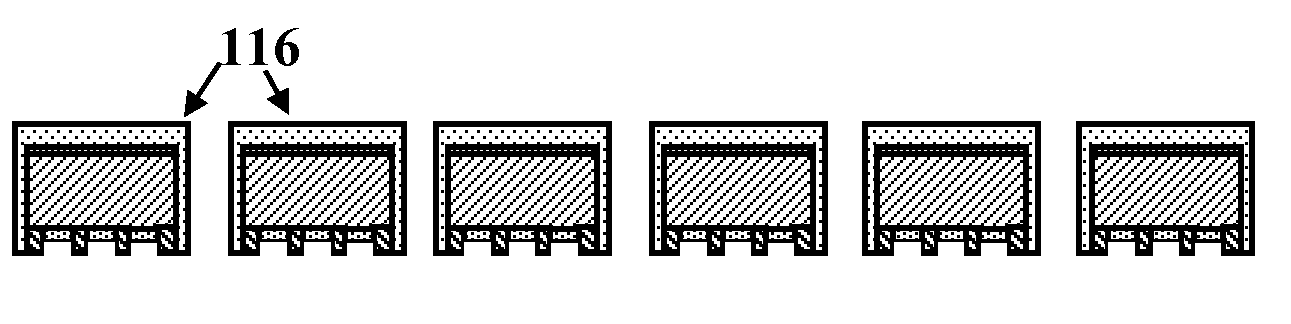
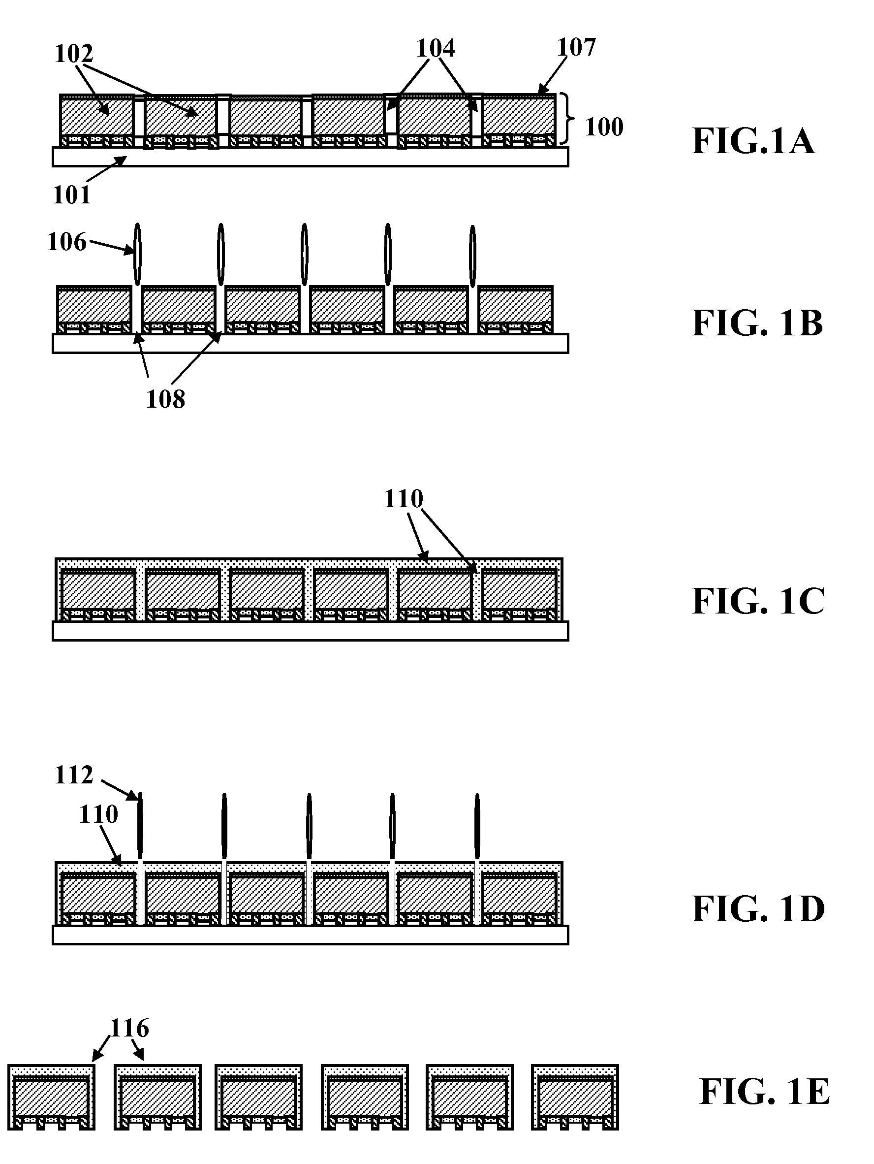
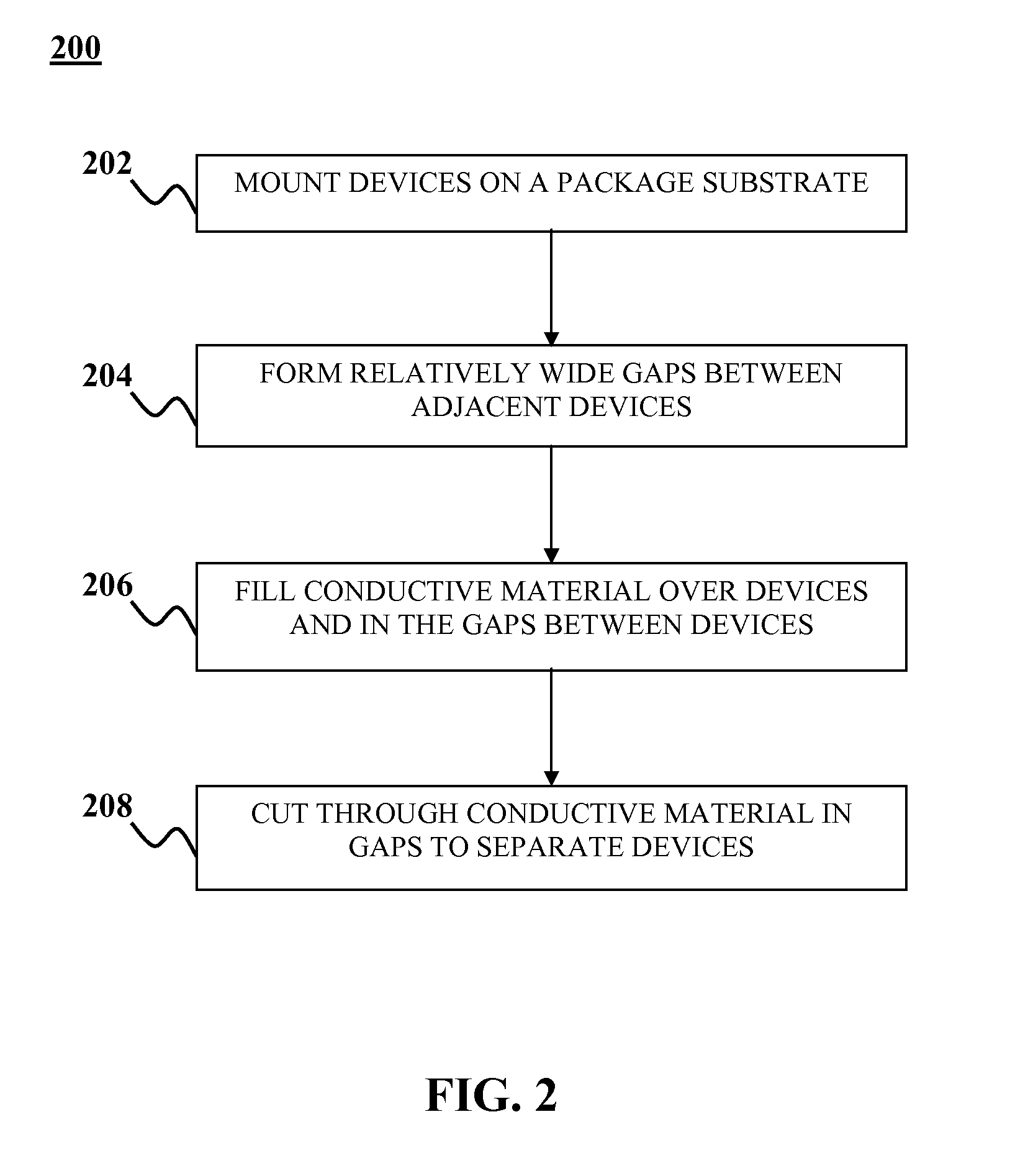
[0015]An example of a process of making electrical interconnections according to an embodiment of the present invention is illustrated in FIGS. 1A-1E and FIG. 2. FIGS. 1A-1E are a sequence of schematic diagrams illustrating a process 200 outlined in the flow diagram of FIG. 2 In this example, electrical interconnections are made at a drain side of trench MOSFETS in a wafer level chip scale package (CSP).

[0016]Referring to FIG. 2, the method 200 may begin at 202 by mounting devices on a package substrate. For example, as shown in FIG. 1A, a...


PUM


Abstract

A method for making back-to-front electrical connections in a wafer level chip scale packaging process is disclosed. A wafer containing a plurality of semiconductor chips is mounted on a package substrate. Each semiconductor chip in the plurality includes one or more electrodes on an exposed back side. Scribe lines between two or more adjacent chips on the wafer are removed to form relatively wide gaps. A conductive material is applied to the back side of the semiconductor chips and in the gaps. The conductive material in the gaps between two or more of the chips is then cut through leaving conductive material on the back side and on side walls of the two or more chips. As a result, the conductive material provides an electrical connection from the electrode on the back side of the chip to the front side of the chip.

Description

FIELD OF THE INVENTION[0001]This invention relates to semiconductor packaging and more specifically relates to a low cost process of wafer level chip scale package (CSP).BACKGROUND OF THE INVENTION[0002]A low package resistance Rds-on and good performance is often desirable for semiconductor devices. This is particularly the case for metal oxide silicon field effect transistor (MOSFET) devices, especially vertical conduction power MOSFET devices having a gate and source electrode on one surface and a drain electrode on the opposite surface. It is also generally desirable to have simple, quick and efficient methods of packaging semiconductor devices. Thus, numerous packaging concepts and methods have been developed in the prior art.[0003]While silicon process technology has advanced significantly in the past decade, for the most part, the same decades-old package technology continues as the primary packaging means. Epoxy or solder die attach along with aluminum or gold wire bonding t...

Claims


Application Information

Patent Timeline
IPC IPC(8): H01L23/06H01L21/304
CPCH01L21/568H01L21/6835H01L2924/1305H01L2924/1306H01L2224/0401H01L24/02H01L24/11H01L24/17H01L2221/68354H01L2224/0231H01L2224/04042H01L2224/13099H01L2224/16H01L2924/01005H01L2924/01013H01L2924/01014H01L2924/01015H01L2924/01022H01L2924/01028H01L2924/01029H01L2924/01033H01L2924/01047H01L2924/01074H01L2924/01079H01L2924/01082H01L2924/014H01L2924/05042H01L2924/13055H01L2924/13091H01L2924/14H01L2924/30105H01L2924/30107H01L2924/01006H01L2924/01024H01L2924/01072H01L2224/0233H01L2224/0239H01L2924/00H01L24/16H01L2924/351
Inventor SUN, MINGFENG, TAOHEBERT, FRANCOISHO, YUEH-SE
Owner ALPHA & OMEGA SEMICON LTD
Learn More