Electroconductive Bonding Material and Electronic Apparatus
a technology of electroconductive bonding and electronic equipment, which is applied in the manufacture of final products, semiconductor/solid-state devices, and conductors. it can solve the problems of poor conductivity of the intermediate connecting part, thermal shock accompanied by rapid temperature change, and long exposure of the connected structure to high-temperature atmospheres. achieve good bonding strength, accelerate the formation of high-melting-point reaction products, and improve the effect of wettability
- Summary
- Abstract
- Description
- Claims
- Application Information
AI Technical Summary
Benefits of technology
Problems solved by technology
Method used
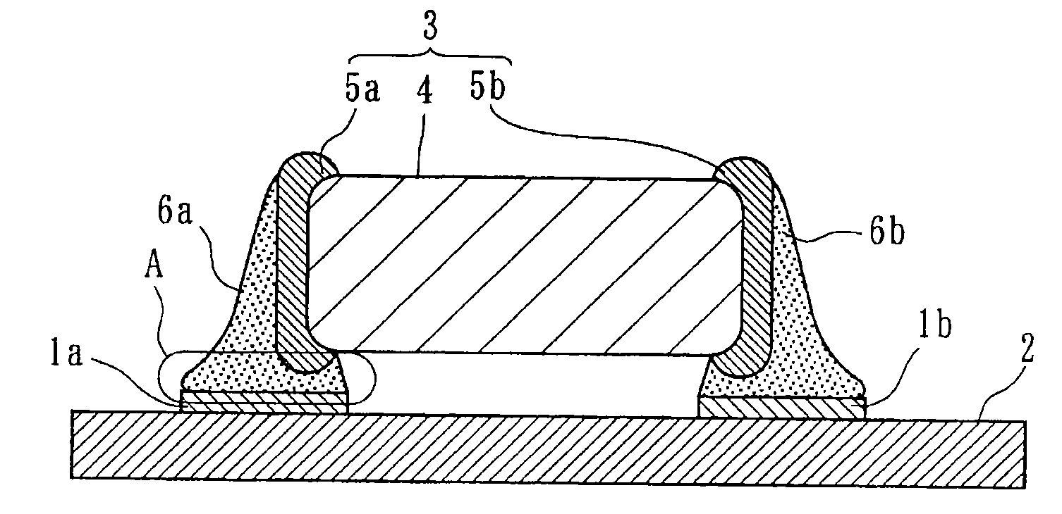
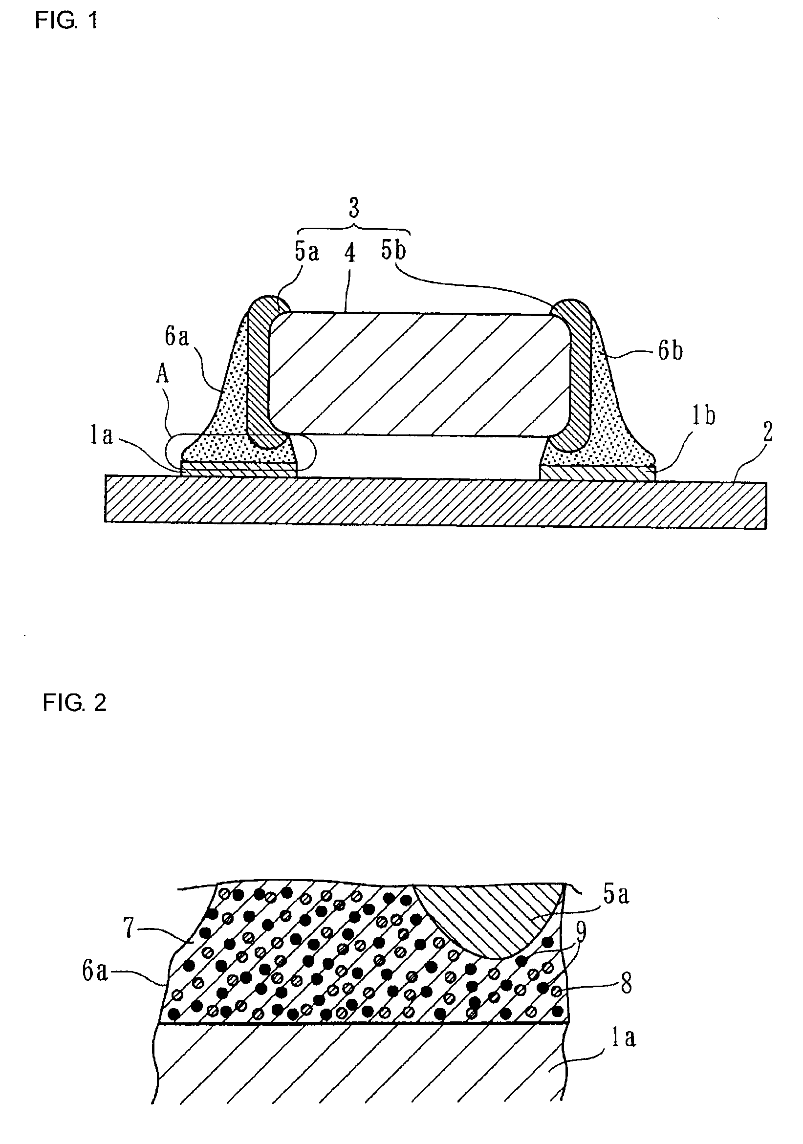
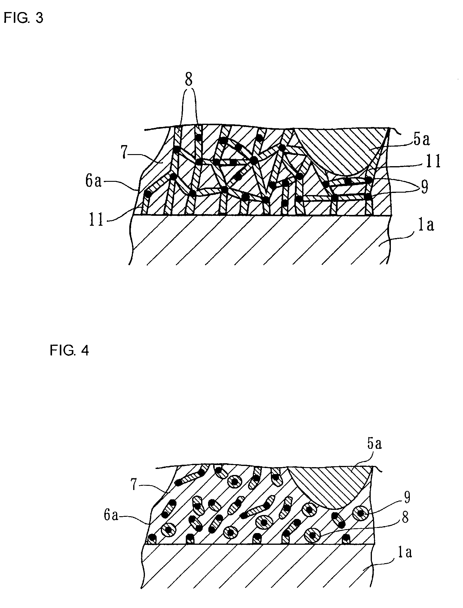
Image

Examples
example 1
Preparation of Electroconductive Bonding Material
[0085]A bisphenol-F type liquid epoxy resin as a thermosetting resin, tert-butyl glycidyl ether as a reactive diluent, an amine compound as a curing agent, a mixture of a boron compound and an epoxy resin as a reaction inhibitor for the curing agent, and succinic acid as a reducing substance were prepared.
[0086]A Sn-58Bi powder (specific gravity: 8.93) (low-melting-point metal powder) having an average particle size D1 of 10 μm and a melting point of 139° C. was prepared, and a Cu powder (specific gravity: 8.75) (high-melting-point metal powder) having an average particle size D2 of 5 μm and a melting point of about 1,080° C. was prepared. The particle size ratio D1 / D2 of the average particle size D1 of the Sn-58Bi powder to the average particle size D2 of the Cu powder was 2.0.
[0087]Next, 25 parts by weight each of tert-butyl glycidyl ether and the amine compound, 12.5 parts by weight of the mixture of the boron compound and the epox...
example 2
[0101]Electroconductive bonding materials of Sample Nos. 11 to 16 were prepared by the same method as in [Example 1] except that, as the high-melting-point powder, Cu powder coated with a Sn layer with a thickness of 0.05 μm (specific gravity: 8.86) (hereinafter referred to as “Sn-coated Cu powder”) was used instead of the Cu powder of Example 1.
[0102]The initial value R0 of connection resistance and the initial value S0 of bonding strength were measured by the same method / procedure as in [Example 1], and furthermore, the rates of change in resistance ΔR1 and ΔR2 and bonding strength S1 and S2 after PCT and after reflow treatment were calculated.
[0103]Table 2 shows the specifications of the electroconductive bonding materials of Sample Nos. 11 to 16 and the test results.
TABLE 2Connection resistanceRate ofAverageRate ofchange inBonding strengthTotalparticleParticlechange inresistanceInitialAfterAftercontentVolumetricsizesizeInitialresistanceaftervaluePCTreflowof metalratio ofSn—58BiC...
example 3
[0109]Using Sn-58Bi powder (specific gravity: 8.93) as low-melting-point metal powder, and using Sn-coated Cn powder (specific gravity: 8.86) as high-melting-point metal powder, electroconductive bonding materials of Sample Nos. 21 to 25 were prepared by the same method as in [Example 1], the electroconductive bonding materials having different particle size ratios D1 / D2 in the range of 0.2 to 10.0.
[0110]The initial value R0 of connection resistance and the initial value S0 of bonding strength were measured by the same method / procedure as in [Example 1], and furthermore, the rates of change in resistance ΔR1 and ΔR2 and bonding strength S1 and S2 after PCT and after reflow treatment were calculated.
[0111]Table 3 shows the specifications of the electroconductive bonding materials of Sample Nos. 21 to 25 and the test results.
TABLE 3Connection resistanceRate ofAverageRate ofchange inBonding strengthTotalparticleParticlechange inresistanceInitialAfterAftercontentVolumetricsizesizeInitia...
PUM
| Property | Measurement | Unit |
|---|---|---|
| Temperature | aaaaa | aaaaa |
| Fraction | aaaaa | aaaaa |
| Fraction | aaaaa | aaaaa |
Abstract
Description
Claims
Application Information
 - R&D
- Intellectual Property
- Life Sciences
- Materials
- Tech Scout
- Unparalleled Data Quality
- Higher Quality Content
- 60% Fewer Hallucinations
Browse by: Latest US Patents, China's latest patents, Technical Efficacy Thesaurus, Application Domain, Technology Topic, Popular Technical Reports.
© 2025 PatSnap. All rights reserved.Legal|Privacy policy|Modern Slavery Act Transparency Statement|Sitemap|About US| Contact US: help@patsnap.com