Method of Forming Conductive Lines and Similar Features

a technology of conductive lines and similar features, applied in the field of digital lithography, can solve the problems of high cost, high processing cost, and disadvantages of each prior art process, and achieve the effects of reducing processing steps, high density, and high profil

Inactive Publication Date: 2009-06-04
PALO ALTO RES CENT INC
View PDF9 Cites 25 Cited by
  • Summary
  • Abstract
  • Description
  • Claims
  • Application Information

AI Technical Summary

Benefits of technology

[0013]Accordingly, the present invention is directed to a method for manufacturing conductive lines (and other features) using a single print-patterned mask structure for etching and material plating. More specifically, the present invention is particularly useful for forming relatively high density, high profile conductive lines on the front or back surface of a solar cell with reduced required processing steps and lower cost as compared to existing process for forming lines, such as photolithography and fired silver / frit.
[0015]It will be appreciated that according to the method of the present invention the print-patterned mask is self-aligning as to the openings in the antireflective layer and the subsequently formed conductive lines. Processing steps are reduced, and the processing that takes place is less likely to damage the photosensitive material substrate, as compared to prior techniques of feature formation. Furthermore, the print-patterned mask may be a relatively tall structure, allowing for the formation of high aspect ratio conductive lines in between the mask structures.

Problems solved by technology

Digital lithography directly deposits material in desired patterns onto a substrate, taking the place of the delicate and time-consuming photolithography processes used in conventional device manufacturing.
However, each of these prior art process have their disadvantages.
For example, the lithographic steps present the disadvantages of: requiring the time needed to perform several pattern and processing steps to etch layers and form the conductive lines; requiring the cost of manufacturing a different reticle for each step; require precise re-registration and alignment from one step to the next; requiring the use of expensive photosensitive resists; and exposing the bulk structure (e.g., crystalline silicon) to extensive handling increasing the risk of damage.
The silver / frit process has the disadvantage of introducing stress on the bulk structure which must be offset by stress applied to the surface opposite from which the silver / frit is applied and producing low, wide (low aspect ratio) conductive lines, which block portions of the photosensitive material from receiving photons (i.e., reducing overall efficiency of the device).
Each of these disadvantages become more pronounced as the trend of wafer size for the photosensitive material to increase continues.

Method used


Image

  • Method of Forming Conductive Lines and Similar Features
  • Method of Forming Conductive Lines and Similar Features
  • Method of Forming Conductive Lines and Similar Features

Examples


first embodiment

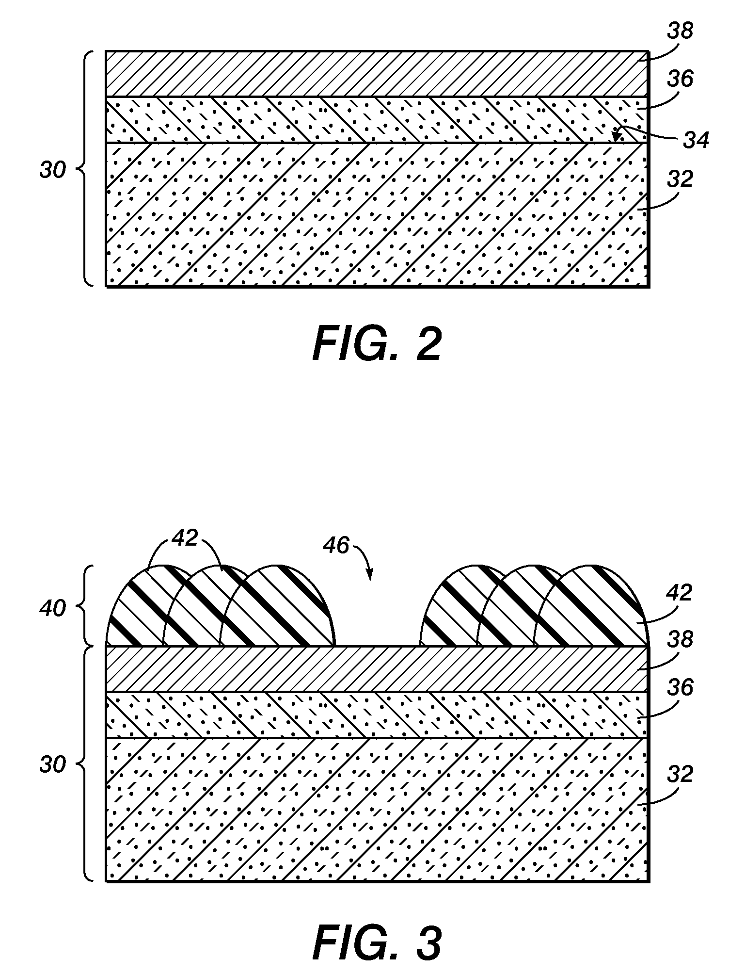
[0035]Described in the following section are specific steps for the formation of a print-patterned mask, and the production of structures formed with said mask. FIGS. 2 through 7 illustrate a device at several intermediate stages of its production according to a process illustrated in FIG. 8. While the following description makes specific reference to the device illustrated in FIGS. 2 through 7, without making more specific reference thereto the description is following the sequence illustrated in FIG. 8.

[0036]With reference to FIG. 2, the process of forming a mask on the front side of photosensitive substrate for the production of conductive lines for a solar cell is illustrated. The process begins with the preparation of the top surface 34 of a single- or poly-crystalline Si (e.g., p-type) substrate 32 for the deposition of various layers thereover. A layer 36 of Si (e.g., n-type) is formed over surface 34 by methods well known in the art. The polarities selected and used in this ...

second embodiment

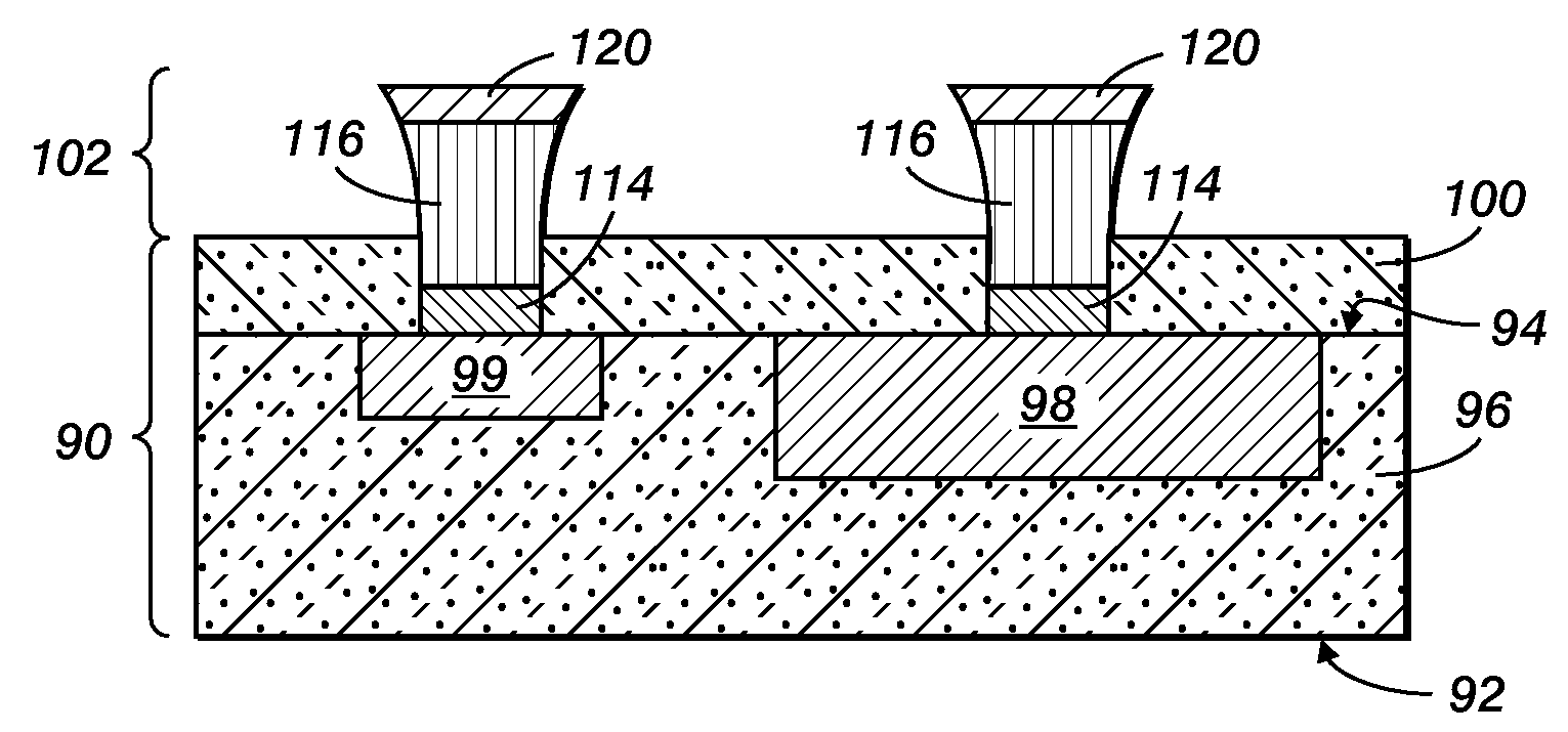
[0048]FIGS. 9 through 14 illustrate a device at several intermediate stages of its production according to a process illustrated in FIG. 15. While the following description makes specific reference to the device illustrated in FIGS. 9 through 14, without making more specific reference thereto the description is following the sequence illustrated in FIG. 15.

[0049]With regard to FIG. 9, there is shown therein a back side structure 90 flipped upside down relative to its final operational orientation. That is, surface 92 is considered the front side of the structure, the side which is oriented toward light in order to receive photons. Processing described hereinbelow therefore is applied to the backside 94 of structure 90.

[0050]Backside structure 90 begins a single- or poly-crystalline Si substrate 96 having a first region 98 of first polarity (e.g., n type) and a second region 99 of second polarity (e.g., p+type) formed therein by methods well known in the art. A passivation / antireflec...


PUM

PropertyMeasurementUnit
Temperatureaaaaaaaaaa
Electrical conductoraaaaaaaaaa
Phaseaaaaaaaaaa

Abstract

A print-patterned structure may be used as a self-aligned etch and deposition mask. A method of forming conductive lines and other similar features over a plurality of layers comprises forming a print-patterned structure over a first layer. The print-patterned structure is used as an etch mask to expose a portion of a second layer. A seed layer is formed over the exposed portion of the second layer, using the print-patterned structure as a deposition mask. Conductive lines or other features may be formed, for example, by electroplating using the seed layer as a contact pad and the print-patterned structure as deposition mask. The present invention is particularly useful in the formation of features for solar cells and the like where the print-patterned structure may be used to form high aspect ratio features.

Description

BACKGROUND OF THE INVENTION[0001]1. Field of the Invention[0002]This invention relates generally to a digital lithography, and more particularly to a printed mask and method of using a single said mask for both etching and plating such as in the fabrication of solar cell devices.[0003]2. Description of the Prior Art[0004]Digital inkjet lithography is a maturing technology designed to reduce the costs associated with photolithographic processes, used often in the fabrication of micro-electronic devices, integrated circuits, and related structures. Digital lithography directly deposits material in desired patterns onto a substrate, taking the place of the delicate and time-consuming photolithography processes used in conventional device manufacturing. One application of digital lithography is the formation of a mask (referred to herein as a “print-patterned mask”) for subsequent processing (e.g., plating, etching, implanting, etc.)[0005]Typically, digital lithography involves depositi...

Claims


Application Information

Patent Timeline
IPC IPC(8): C25D5/02
CPCC25D1/04H01L2924/01072H01L24/02H01L31/022425H01L31/18H01L2224/1147H01L2924/01004H01L2924/01013H01L2924/01014H01L2924/01015H01L2924/01028H01L2924/01029H01L2924/01033H01L2924/01047H01L2924/0105H01L2924/01075H01L2924/01078H01L2924/014H01L2924/05042H01L2924/14H05K3/0076H05K3/061H05K2203/1105Y02E10/50H01L2924/01006C25D5/022H01L2224/0401
Inventor SHRADER, ERICLIMB, SCOTT
Owner PALO ALTO RES CENT INC
Why Eureka
Try Eureka