High performance high capacity memory systems

a memory system and high-capacity technology, applied in the field of high-capacity high-capacity memory systems, can solve the problems of limiting factors, high performance and high capacity conflicting requirements, degradation of performance and/or stability, etc., and achieve the effect of high capacity, low cost and no increase in data signal loading

Inactive Publication Date: 2009-04-23
UNIRAM TECH
View PDF12 Cites 7 Cited by
  • Summary
  • Abstract
  • Description
  • Claims
  • Application Information

AI Technical Summary

Benefits of technology

[0020]The primary objective of this invention is, therefore, to provide high capacity memory systems without increasing the loading of data signals. The other primary objective of this invention is to achieve the above objective with minimum overhead in performance and in cost. Another objective is to achieve the above objectives while using interfaces that are compatible with conventional memory systems. These and other objectives are achieved by using multiplexing to isolate loadings on data signals. The resulting memory systems are capable of achieving high capacity with basically the same performance and power of a single conventional memory. The interface signals also can be compatible with conventional memory systems.

Problems solved by technology

In reality, high performance and high capacity have conflicting requirements that can become limiting factors.
Increase in loading typically means degradation in performance and / or stability.
This problem is especially significant for prior art DDR2 synchronized DRAM with data rate higher than 600 millions of bits per second (MPS) per pin.
DDR2 DRAM uses Stub Series Terminated Logic (SSTL) buses with on-chip terminal resistors so that each memory chip (even when it is not active) is sinking currents through terminal resistors, making it impractical to connect large number of prior art memory modules while operating at high performance.
It is well known that using multiple DDR2 DIMM modules would degrade performance significantly, especially at data rate higher than 600 millions of bits per second (MPS) per pin.
Increasing capacity by adding more and more prior art memory modules is therefore not practical.
Such methods reduce the loading on control signals, but the loading problems in data signals are not solved.
An RDIMM uses PLL to generate local clock and use a “register chip” that comprises latches to buffer control signals; the price to pay for RDIMM approach is one additional clock latency, and the RDIMM approach does not solve loading problems in data signals.
Those existing AMB products are typically complex high cost integrated circuits (IC) comprise more than 600 interface signals.
However, the memory access latency is increase by the need to transfer signals serially through the AMBs connected in daisy chain architecture.
The worst delay time increases linearly with the number of FBDIMM modules linked in the daisy chain, limiting the capability to increase capacity.
In addition, the FBDIMM modules are by far more expensive than conventional memory modules, and they are not compatible with conventional memory interfaces, limiting their application on high cost server or work stations.
FBDIMM saves power by isolating memory chips in different modules, but the power consumed by overhead in AMB is significant.
Such method can increase the capacity of a single memory module, but it does not help to allow multiple modules working on the same system.
The added delay in terms of clock latency can degraded system performance.
The increase in capacity is limited by the space of individual module.

Method used


Image

  • High performance high capacity memory systems
  • High performance high capacity memory systems
  • High performance high capacity memory systems

Examples


Embodiment Construction

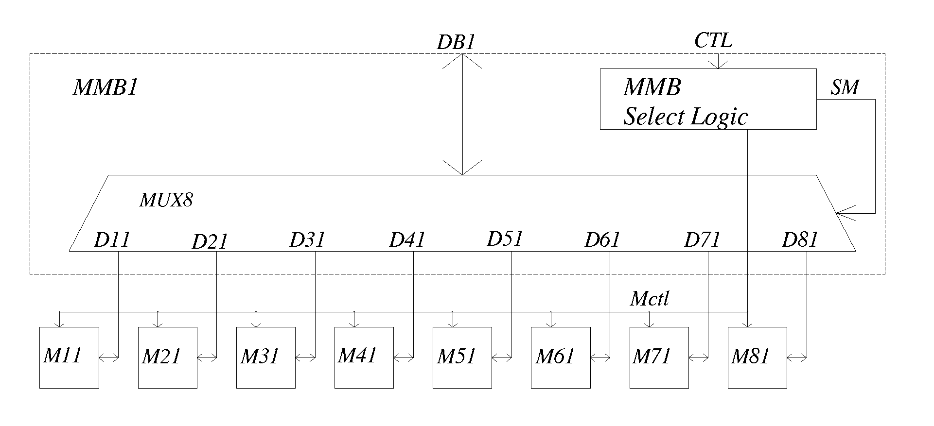
[0035]FIG. 3(a) is a simplified schematic block diagram for one example of the Multiplexed Memory Buffer (MMB) module of the present invention. In this example, the MMB memory module (MMB1) comprises 8 memory chips (M11, M21, M31, M41, M51, M61, M71, M81). Comparing to the prior art memory module in FIG. 1(a), the key difference is that the memory chips (M11-M18) in the prior art memory module is arranged in parallel data connection to support a complete set of system data signals (DB1-DB8). In contrast, the memory chips (M11, M21, M31, M41, M51, M61, M71, M81) in memory modules of the present invention is arranged to support a sub set (DB1) of the system data signals, while the first memory chip (M11) supports DB1, the second memory chip (M21) supports DB1, and the eighth memory chip (M81) also supports DB1. In other words, all those memory chips (M11, M21, M31, M41, M51, M61, M71, M81) are arranged to support the same data signals (DB1). The functions of those memory chips are equ...


PUM


Abstract

The present invention provides memory system architectures developed to increase the capacity of memory systems. Typically applications including the main memory of computers. Memory systems of the present invention can achieve capacities larger than prior art systems by one or two orders of magnitudes without significant degradation in performance while using system interfaces that are compatible with existing memory systems with no or minimal modifications.

Description

[0001]This application is a continuation-in-part application of previous patent application with a Ser. No. 11 / 933,556 with the same title and filed on Nov. 1, 2007. The Ser. No. 11 / 933,556 application is a continuation-in-part application of previous patent application with a Ser. No. 11 / 874,914 with the same title and filed on Oct. 19, 2007.DESCRIPTIONBackground of the Invention[0002]The present invention relates to structures and methods designed to increase the capacity of high performance memory systems.[0003]The present invention is applicable to most types of memories such as dynamic random access memory (DRAM), static random access memory (SRAM), nonvolatile memories, etc. Among the wide varieties of possible applications, the most well known applications are the main memory in computers. We will focus on computer main memory using double data rate version 2 (DDR2) dynamic random access memories (DRAM) as examples to demonstrate the basic principles of the present invention....

Claims


Application Information

Patent Timeline
Patent Type & Authority Applications(United States)
IPC IPC(8): G11C7/10
CPCG11C7/1066G11C7/22G11C11/4093G11C11/4076G11C7/222
Inventor SHAU, JENG-JYE
Owner UNIRAM TECH
Why Eureka
Try Eureka