Resin Composition for Optical Material, Resin Film for Optical Material and Optical Waveguide Using Same

a technology of optical material and resin film, which is applied in the direction of optical elements, photomechanical devices, instruments, etc., can solve the problems of difficult to realize a thickness of about 50 m, poor film thickness precision, and difficult to perform film formation on electric printed wiring boards. , to achieve the effect of high transparency, high heat resistance and high transparency

Inactive Publication Date: 2008-10-23
HITACHI CHEM CO LTD
View PDF6 Cites 28 Cited by
  • Summary
  • Abstract
  • Description
  • Claims
  • Application Information

AI Technical Summary

Benefits of technology

[0021]In view of the above-mentioned problems, it is an object of the present invention to provide a resin composition for an optical material that allows formation of a thick film having high transparency, high heat resistance, and high precision and has high productivity and that is particularly useful for resin films for forming optical waveguides, a resin film for an optical material using such a resin composition, and an optical waveguide using such a film. It is another object of the present invention to provide a flexible optical waveguide having high flexibility and toughness and in addition having excellent productivity and a method of producing the same.
[0067]The resin composition for an optical material of the present invention has high transparency and high heat resistance. The resin film for an optical material including the composition has high transparency and high heat resistance and allows for high-precision formation of a thick film. Further, use of the resin film for an optical material enables production of optical waveguides having excellent performance with high productivity.

Problems solved by technology

However, when materials for waveguides including, for example, deuterized silicone resins or fluorinated polyimides are used, there arises a problem in that it is difficult to realize a thickness of about 50 μm on an optical / electronic board or, if it is possible to realize, precision of film thickness will be poor because the materials for waveguides are generally include solvents having low viscosities although the resins themselves have high heat resistance to endure about 300° C.
Further, when fluorinated polyimide waveguide materials, which themselves have high heat resistance to endure about 300° C. and high transparency as high as 0.3 dB / cm at a wavelength of 850 nm, are used, film formation on an electric printed wiring board was difficult to be performed since film formation requires heating at 300° C. or more for several tens minutes to several hours.
Further, fluorinated polyimides have no photosensitivity, so the method of fabricating optical waveguides by exposure to light and development can not be applied thereto, and they thus have poor productivity and poor applicability to large-area fabrication.
Further, since optical waveguides are fabricated by a film forming method that involves applying a liquid material on a substrate, management of film thickness is cumbersome and in addition, the resin applied on the substrate is still liquid before curing, so the resin will flow on the substrate to make it difficult to maintain uniformity of film thickness.
Thus, there are many problems arising from the fact that the form of the material is liquid.
However, when liquid waveguide materials are used for the upper cladding, there tends to occur unevenness as a result of following up the ridge pattern of the core, so it is difficult to realize flatness.
The epoxy resins have problems similar to those of the above-mentioned waveguide materials including deuterized silicone resins or fluorinated polyimides because the epoxy resins are liquid.
These epoxy resins have excellent transparency and heat resistance at about 200 to 280° C. However, since an epoxy resin is used for fabricating optical waveguides by applying a liquid material on a substrate and forming a film by, for example, a spin coating method, management of film thickness is cumbersome and in addition, the resin applied on the substrate is still liquid before curing, so the resin will flow on the substrate to make it difficult to maintain uniformity of film thickness.
Thus, there are many problems arising from the fact that the form of the material is liquid.
Further, in high speed, high-density signal transmission, between electronic devices or printed wiring boards, transmission through the conventional electric wiring is approaching to a limit of attaining high speed and high density due to restrictions of mutual interference and attenuation of signals.
This method takes much time for forming each layer and in addition has problems arising from the fact that the form of the material is liquid.
That is, since optical waveguides are fabricated by a film forming method that involves applying a liquid material on a substrate, management of film thickness is cumbersome and in addition, the resin applied on the substrate is still liquid before curing, so the resin will flow on the substrate to make it difficult to maintain uniformity of film thickness.
Also, the method is not suitable for mass production of optical waveguides having a size of 10 cm or more because of use of silicon for substrates.
Further, the above-mentioned production method involves a step of dry etching, which is a high vacuum process, so dry etching must be performed for a very long period of time to fabricate multi-mode optical waveguides having a thick core layer.

Method used


Image

  • Resin Composition for Optical Material, Resin Film for Optical Material and Optical Waveguide Using Same
  • Resin Composition for Optical Material, Resin Film for Optical Material and Optical Waveguide Using Same
  • Resin Composition for Optical Material, Resin Film for Optical Material and Optical Waveguide Using Same

Examples


example 1

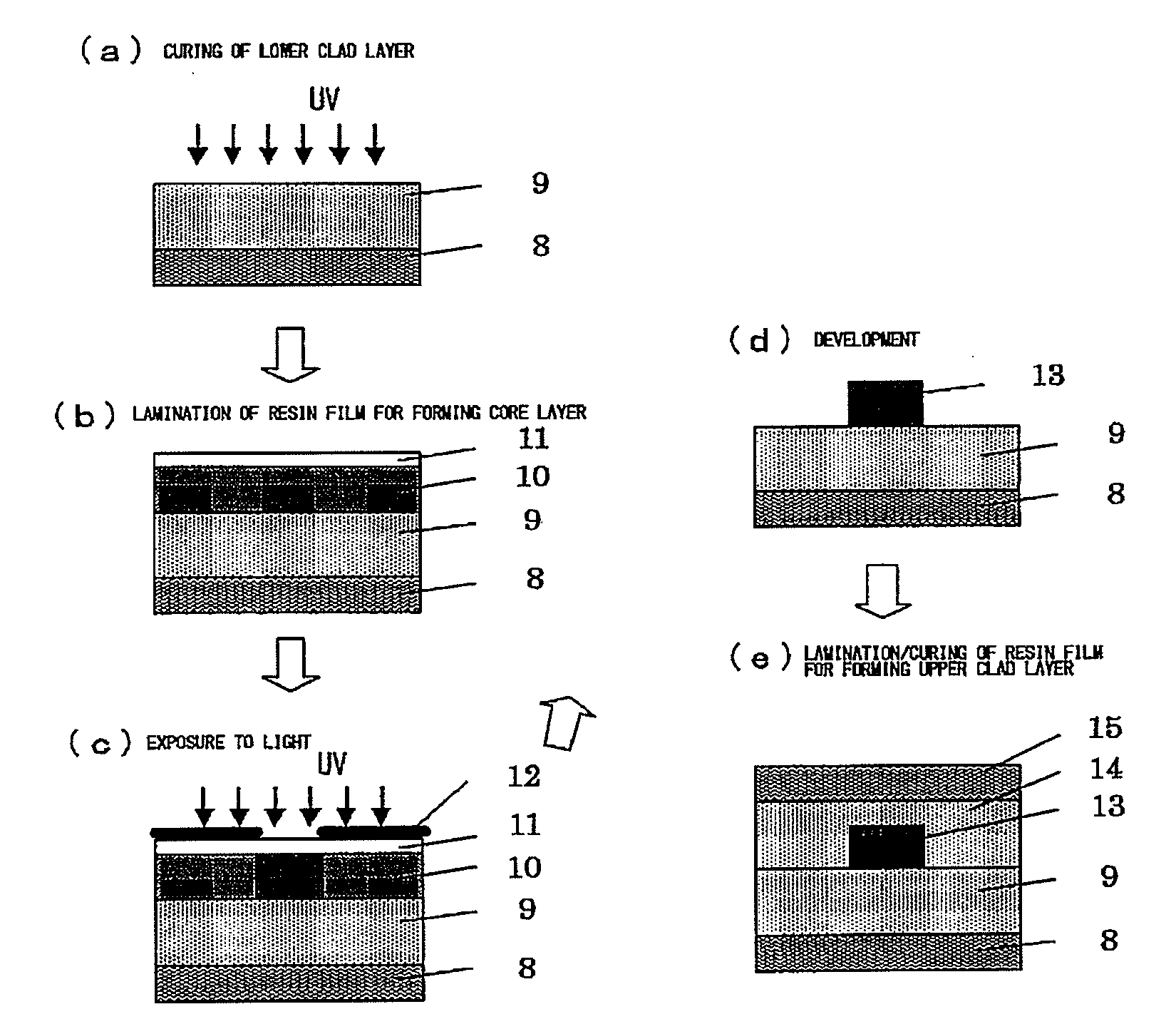
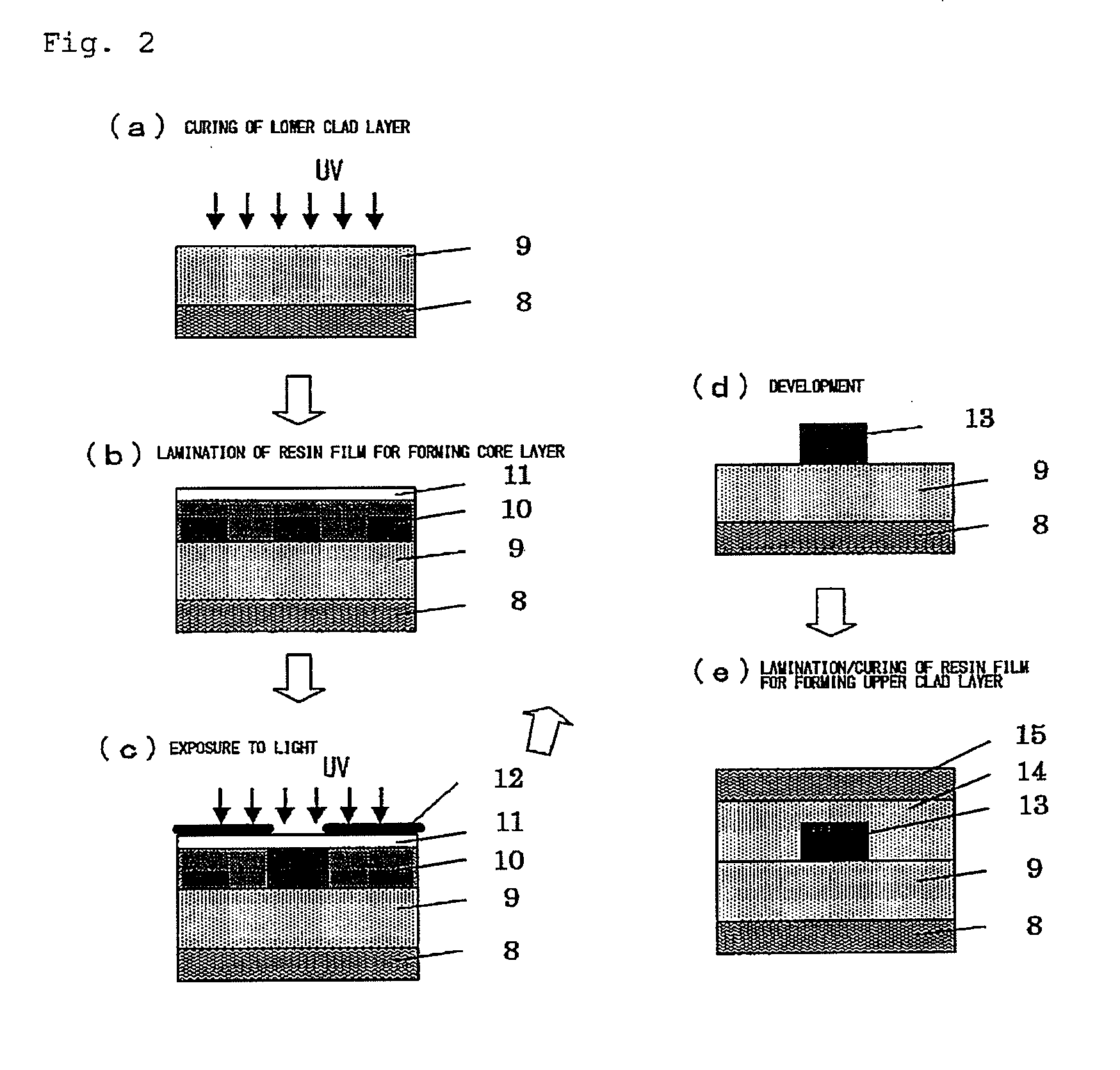
[0173]Epoxyacrylate oligomer (trade name “HITALLOID”, manufactured by Hitachi Chemical Co., Ltd.) and phenoxy resin (trade name “YP-50”, manufactured by Tohto Kasei Co., Ltd.) were blended in equivalent mass ratio (using 50 mass parts per 100 mass parts of total resin of methyl ethyl ketone as a solvent). To this was added a three-component optical radical generator consisting of an optical initiator (2,2-bis(2-chlorophenyl)-4,4′,5,5′-tetraphenyl 1,2′-biimidazole manufactured by Tokyo Chemical Industry Co., Ltd.; 4,4′-bis(diethylamino) benzophenone manufactured by Tokyo Chemical Industry Co., Ltd., and 2-mercaptobenzimidazole manufactured by Tokyo Chemical Industry Co., Ltd.) in an amount of 2 mass parts based on 98 mass parts of total resin to provide a resin composition for forming an optical waveguide. This was applied on a PET film (“A4100”, manufactured by Toyobo Co., Ltd.) using an applicator (“YBA-4”, manufactured by Yoshimitsu Seiki Co., Ltd.) and dried under conditions of 8...

example 2

[0177]A resin film for forming optical waveguides was obtained in the same manner as that in Example 1 except that solid epoxy resin (trade name “Epototo YD-7020”, manufactured by Tohto Kasei Co., Ltd.) was used in place of the phenoxy resin. The thickness of the film was 12 μm.

[0178]The resin film for forming optical waveguides was treated in the same manner as in Example 1 to obtain a slab optical waveguide (core thickness 12 μm). The refractive index of the slab optical waveguide (core) was measured in the same manner as in Example 1. As a result, the refractive index was 1.565 for both TE polarized light and TM polarized light. This was passed through a solder reflow oven (“Salamander”, manufactured by Furukawa Electric Co., Ltd.) three times under conditions of a maximum temperature of 265° C. (retention time of 15 to 20 seconds at 260° C. or more) and nitrogen atmosphere.

[0179]Transmission losses before and after reflow were measured using a prism coupler optical characteristi...

example 3

[0181]A resin film for forming optical waveguides was obtained in the same manner as that in Example 1 except that acryl acrylate oligomer (trade name “HITALLOID 7975”, manufactured by Hitachi Chemical Co., Ltd.) was used in place of epoxyacrylate oligomer, and acrylic resin (trade name “HTR-860P-3DR”, manufactured by Teikoku Chemical Industries Co., Ltd.) was used in place of phenoxy resin. The thickness of the film was 12 μm.

[0182]The resin film for forming optical waveguides was treated in the same manner as in Example 1 to obtain a slab optical waveguide (core thickness 12 μm). The refractive index of the slab optical waveguide (core) was measured in the same manner as in Example 1. As a result, the refractive index was 1.505 for both TE polarized light and TM polarized light. This was passed through a solder reflow oven (“Salamander”, manufactured by Furukawa Electric Co., Ltd.) three times under conditions of a maximum temperature of 265° C. (retention time of 15 to 20 seconds...


PUM

PropertyMeasurementUnit
Percent by massaaaaaaaaaa

Abstract

Disclosed is a resin composition for an optical material which contains a base polymer (A), a photopolymerizable compound (B), and a photopolymerization initiator (C). Also disclosed is a resin film for an optical material which is made of such a resin composition for an optical material. Specifically disclosed is a resin composition for an optical material which has high transparency and high heat resistance, while enabling formation of a thick film with high precision. This resin composition is particularly useful for a resin film which is used for forming optical waveguides. Also specifically disclosed are a resin film for an optical material using such a resin composition and an optical waveguide using such a resin film.

Description

TECHNICAL FIELD[0001]The present invention relates to a resin composition for an optical material having excellent heat resistance, transparency, and productivity, a resin film for an optical material, and an optical waveguide using the film as well as to a flexible optical waveguide having excellent flexibility, toughness, and productivity and to a method of producing the same.BACKGROUND ART[0002]To cope with an increase in volume of information concomitant with popularization of the Internet and Local Area Network (LAN), optical interconnection technology that uses optical signals is being under development not only in communication fields of main line and access type but also in short distance signal transmission between boards or inboards of routers and server devices. Specifically, to enable use of light in short distance signal transmission between boards or in boards in routers and server devices, optical / electronic boards that include an electric printed wiring board and an ...

Claims


Application Information

Patent Timeline
IPC IPC(8): G02B6/10C08F2/46
CPCC08F2/50C08L33/062C08L33/068C08L63/10C08L71/12G02B6/138G03F7/027G03F7/032C08L2666/02C08L2666/22C08F2/44G02B1/045C08F220/28C08J5/18
Inventor SHIBATA, TOMOAKIMAKINO, TATSUYAOCHIAI, MASAMITAKAHASHI, ATSUSHITAKASAKI, TOSHIHIKO
Owner HITACHI CHEM CO LTD
Why Eureka
Try Eureka