Soft error rate calculation method and program, integrated circuit design method and apparatus, and integrated circuit

a technology of integrated circuit and error rate calculation, applied in error detection/correction, instruments, computing, etc., can solve problems such as soft error, serious problems, and “inversion” of information, and achieve the effect of satisfying specification and easy estimation

Inactive Publication Date: 2008-10-16
RENESAS ELECTRONICS CORP
View PDF7 Cites 4 Cited by
  • Summary
  • Abstract
  • Description
  • Claims
  • Application Information

AI Technical Summary

Benefits of technology

[0016]According to this embodiment, if a soft error rate that is estimated by deriving the second mathematical expression from an actually measured soft error rate and substituting a desired node voltage or diffusion layer area into the second mathematical expression is equal to or larger than a prescribed value, the method makes a design change and recalculates a soft error rate, thereby designing a semiconductor integrated circuit that satisfies the specification of a soft error rate. The present invention thus enables easy estimation of a soft error rate SER in SRAM or a storage circuit element during the product design phase.

Problems solved by technology

A soft error is one of the problems caused by scaling process of recent semiconductor devices.
In a narrow sense, a soft error of semiconductor devices is a temporal defect that causes the “inversion” of information due to the loss of charges that are accumulated in a storage node by radiation.
Combined with the trend for low-voltage circuit design, the soft error will become a serious problem.
However, with the recent development of small memory cells, it is difficult to add a large capacitance in a simple process.
In addition, it is unable to add a capacitance that is large enough to prevent soft errors to a high-speed SRAM because of the operation speed.
However, a considerable amount of prototyping is required to determine the optimization conditions.
Therefore, a soft error rate SER cannot be determined until prototyping a product or TEG (Test Element Group).
Generally, the soft error simulation requires product process information, mask layout information, circuit information, nuclear reaction model and soon, and therefore there is a problem that it is only engineers with a good knowledge of a simulator (i.e. those who developed a simulator) who can use the simulator.

Method used


Image

  • Soft error rate calculation method and program, integrated circuit design method and apparatus, and integrated circuit
  • Soft error rate calculation method and program, integrated circuit design method and apparatus, and integrated circuit
  • Soft error rate calculation method and program, integrated circuit design method and apparatus, and integrated circuit

Examples


first embodiment

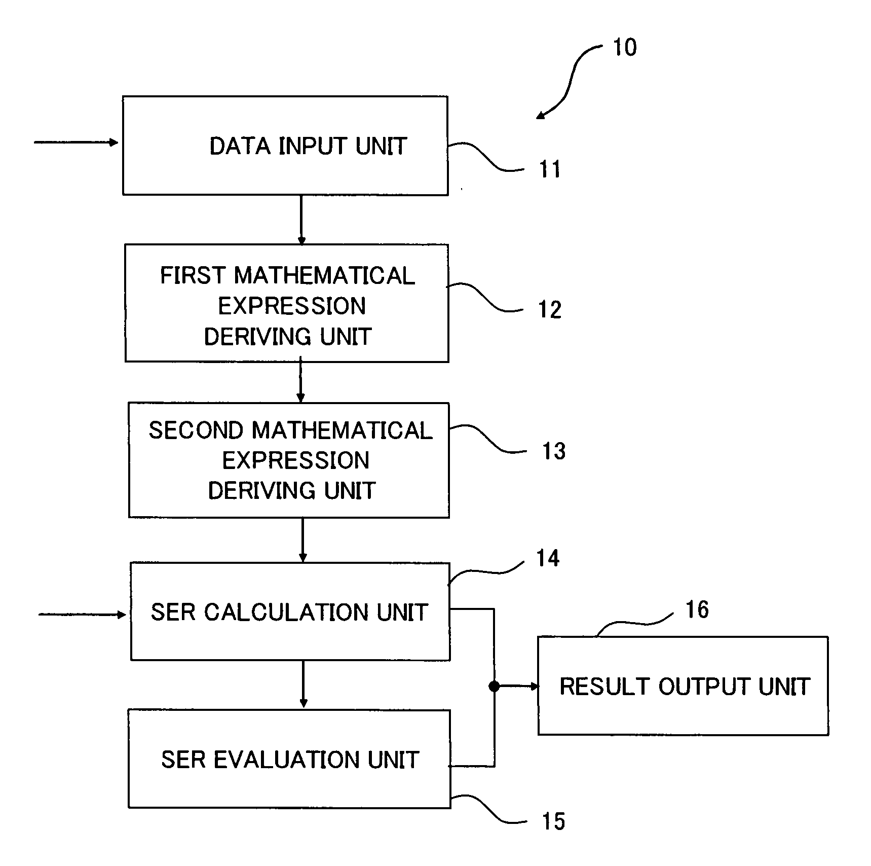
[0062]A first embodiment of the present invention is described hereinafter. FIG. 4 is a view showing a semiconductor device design apparatus according to this embodiment. The design apparatus is configured to design a semiconductor device that includes a storage circuit or an information holding circuit which is composed of a transistor such as MISFET. Referring to FIG. 4, a semiconductor device design apparatus 10 includes a data input unit 11 to input a SER measurement result, first and second mathematical expression deriving units 12 and 13, a SER calculation unit 14 to estimate SER of a semiconductor device from the second mathematical expression, a SER evaluation unit 15 to evaluate a SER estimation result, and a result output unit 16 to output a SER estimation result or the like.

[0063]The data input unit 11 inputs a measurement result of a relationship between a soft error rate and an information storage node diffusion layer area of a storage circuit or an information holding ...

second embodiment

[0081]A second embodiment of the present invention is described hereinafter. As described in the first embodiment, it is possible to estimate SER in the phase of designing a semiconductor device, thereby enabling design change according to the estimation result, thus enabling measures against soft errors. The measures against soft errors involve adding a capacitor (which is referred to hereinafter as an additional capacitor) to a storage node of a cell transistor, replacing a substrate with SOI, and so on.

[0082]The SER estimation method in the first embodiment is applicable regardless of some difference in process because it uses data of a plurality of cells with the relationship close to general scaling. However, when an additional capacitor is added to an information storage node or when a SOI substrate is used, SER exhibits a different tendency from a previous-generation; as a result, the above-described estimation method cannot be used simply in some cases. This embodiment enabl...

third embodiment

[0102]As described in the above embodiments, the SER estimation method of the present invention enables the estimation of SER of SRAM, and further it is applicable to various cell structures. This embodiment provides a SER estimation method that is particularly suitable for use in the circuit configuration different from SRAM. The case where the present invention is applied to a F / F circuit, a latch circuit or the like including an inverter composed of pMISFET and nMISFET, which is different from a SRAM cell, is described hereinbelow.

[0103]Generally, a F / F circuit and a latch circuit have a different size ratio of pMISFET and nMISFET and a different diffusion layer interval from those of SRAM. In such a case, an expression that accurately approximates measurement data cannot be derived for some actually-measured circuits.

[0104]H. Fukui et al., “Comprehensive Study on Layout Dependence of Soft Errors in CMOS Latch Circuits and Its Scaling Trend for 65 nm Technology Node and Beyond”, ...


PUM


Abstract

A first mathematical expression indicating a dependence of SER on an information storage node diffusion layer area at the same information storage node voltage Vn is derived with a use of a result of measuring a relationship between SER and the information storage node diffusion layer area of a storage circuit or an information holding circuit composed of MISFET using a plurality of information storage node voltages Vn as a parameter. Then, a second mathematical expression is derived from the measurement result by substituting a relationship indicating a dependence of SER on an information storage node voltage at the same information storage node diffusion layer area Sc into the first mathematical expression. SER can be calculated by substituting a desired information storage node diffusion layer area and a desired information storage node voltage of a storage circuit or an information holding circuit into the second mathematical expression.

Description

BACKGROUND OF THE INVENTION[0001]1. Field of the Invention[0002]The present invention relates to a semiconductor integrated circuit including a storage circuit or an information holding circuit composed of a transistor, a soft error rate calculation method and a program of the same, and a design method and a design apparatus of the same.[0003]2. Description of Related Art[0004]A soft error is one of the problems caused by scaling process of recent semiconductor devices. In a narrow sense, a soft error of semiconductor devices is a temporal defect that causes the “inversion” of information due to the loss of charges that are accumulated in a storage node by radiation. Combined with the trend for low-voltage circuit design, the soft error will become a serious problem.[0005]One measure against this problem is to improve the resistance to soft errors by adding a capacitance to a storage node. However, with the recent development of small memory cells, it is difficult to add a large cap...

Claims


Application Information

Patent Timeline
Patent Type & Authority Applications(United States)
IPC IPC(8): G06F11/00
CPCG06F17/5036G06F30/367
Inventor FURUTA, HIROSHIMONDEN, JUNJIMIZUGUCHI, ICHIRO
Owner RENESAS ELECTRONICS CORP
Why Eureka
Try Eureka