This method has a primary
disadvantage that the exposed copper is etched sideward when it is etched downwards during
etching.
As a result, it is difficult to form wires, thus limiting application of the subtractive method in forming fine lines.
Therefore, it has a
disadvantage of high cost, and it has not been perfect yet.
However, when comparing with the semi-additive method described above, the ability of the modified semi-additive method to form fine lines is still limited, because the copper layer obtained by plating has a thickness greater than that of the copper layer obtained by
electroless plating.
But it is limited by its limited ability to form fine lines.
Therefore, it has a
disadvantage of high cost, and it is still not perfect yet.
(1) Mechanical perforation, which is the conventional method for forming conductive through holes. For example, the desired through holes are formed in a substrate through a punch or a
drill press, and then hollow conductive through holes are formed by depositing or plating copper. Referring to FIG. 4, reference number 41 refers to a substrate, reference number 42 refers to a lower layer of wires, reference number 43 refers to a
dielectric layer, reference number 44 refers to a hollow conductive through hole, and reference number 45 refers to an upper layer of wires. The aperture has a greater
diameter when formed by the mechanical perforation. Therefore, it is difficult to increase the density of wires.
(2)
Optical imaging dielectric or
laser perforation technique for forming blind conductive vias. The method for forming blind conductive vias comprises the following steps: forming micro-dents on photo-sensitive dielectric materials by an image-
transfer technique, or forming micro-dents directly on dielectric materials by a
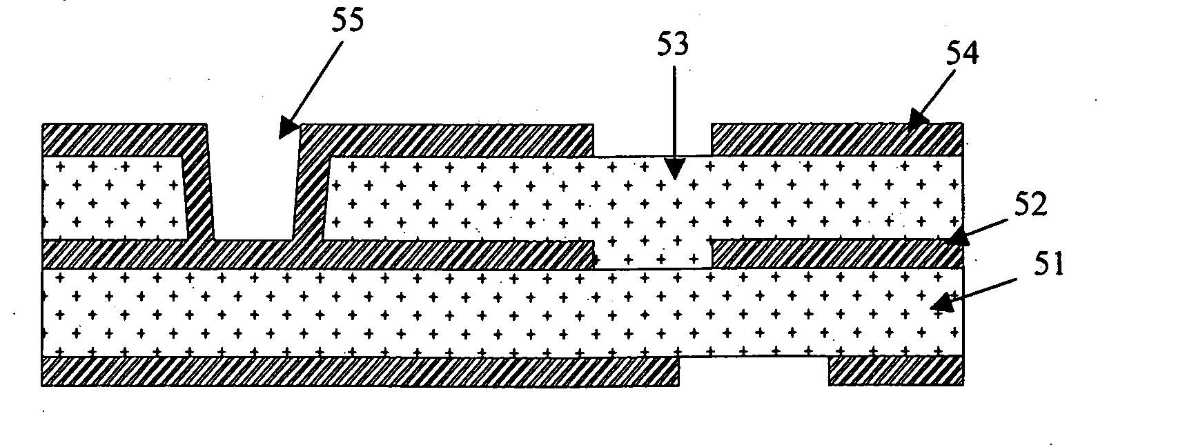
laser perforation technique; and then forming blind conductive vias by depositing or plating copper, as described in FIG. 5 (wherein, 51-a substrate, 52-a lower layer of wires, 53-a dielectrics layer, 54-an upper layer of wires, and 55-a blind conductive vias). The method forms hollow conductive vias. However, the
conductivity,
thermal conductivity and reliability of the hollow conductive vias are lower than those of solid blind vias. At the same time, this structure cannot provide stacked via structure, therefore, it is difficult to increase the density of wires.
(3) Japanese patent No. 6-314878 discloses a method of wholely conducting a lower wire layer and forming a
resist pattern having an opening portion and depositing
metal on a concave section of the
resist pattern by means electrolytic plating to form a pillar conductor. However, the method has a problem that the height of the pillar conductor is easily non-uniform. At the same time, the plating
current density can not be heightened, so the formation of the pillar takes a long time.
(4) U.S. Pat. No. 6,555,209B1 discloses a method of forming solid conductor, comprising:
coating a
etching-resistance
metal on the lower wiring layer; forming a plating layer above the said protective
metal by electrolytic plating; forming a
mask layer on the surface of the plating layer where pillar-like metallic body is formed;
etching the said plating layer to form the pillar; etching the protective metallic layer to get the lower layer pattern. However, the method has the next disadvantage. The
diameter of the connection pillar with a certain height is smaller than the bottom portion because of the end portion because of the etching factor, which makes it difficult to narrow the gap between the connection pillar needed to form a fine circuit pattern. And so the method is still limited to increase the wire density.
(5)
Copper filling plating for forming conductive vias, comprising: forming micro-dents on photo-sensitive dielectric materials by an image-
transfer technique, or forming micro-dents, directly on dielectric materials by a
laser perforation technique; and then forming blind conductive vias by depositing or plating copper. During the process of plating, not only the copper layer is thickened, but also the vias is filled by filling-vias techniques. This method can provide stacked via structure easily and can produce the conductive vias with high reliability. However, in the practical process of plating, the copper layer generally has a greater thickness in order to fill the vias and the wires are formed by subtractive method, which is disadvantage for the preparation of fine lines.
However, the conventional semi-additive method cannot provide solid conductive vias, thereby cannot provide stacked vias to connect any
layers.
But the methods still have many disadvantages as described above or are not compatible with the semi-additive process.
