
Optical transceiver integratable with silicon VLSI

a transceiver and integrated technology, applied in the field of optical transceivers, can solve the problems of electrical interconnects that cannot meet the requirements of data integrity, and high speed interconnects that are subject to the trade-off between distance and bit rate,

Inactive Publication Date: 2008-04-10
RGT UNIV OF CALIFORNIA
View PDF3 Cites 10 Cited by
  • Summary
  • Abstract
  • Description
  • Claims
  • Application Information

AI Technical Summary

Benefits of technology

[0025] Since the modulator of the present invention is based on field effect as opposed to current injection, it allows for low power operation and eliminates the need for high current drive in a high-speed driver circuitry, greatly reducing that part of the “overhead”.
[0027] The modulator structure of the present invention can be easily fabricated on any conductive layer with a smooth surface, such as a doped silicon substrate, the output metal pads of a finished very large scale integration (VLSI) chip, and a glass wafer with FO coating layer. Thus, it is suitable for silicon-based optical interconnects and low cost optical communication.
[0030] The advantages of such a transceiver include easy integration with Si IC resulting in minimum intrusion to conventional Si IC processing, and low “overhead” during electronic-optical signal conversion. Because the transmitter is based on light modulation rather than emission, the chip power consumption is significantly lowered. Furthermore, both the modulator and the detector of the present invention can be fabricated during conventional CMOS backend processing, making it more likely to be accepted by the IC industry, and an ideal low cost optical transceiver that is missing in today's fiber-optic communication infrastructure.
[0036] In addition, the vertical cavity may be configured to amplify a small change in absorption of the EA layer to a significantly higher contrast in the reflectivity of the modulator.
[0046] In one mode of the current embodiment, the saturation intensity of the optically absorptive layer effects an overall reflectivity of the cavity to modulate the optical signal.

Problems solved by technology

One of the major technological challenges facing the industry today is high data rate (or for analog applications, high bandwidth) communication between chips.
As the data rate increases to above Gbps, the ability of maintaining the data integrity using electrical interconnects becomes a very challenging issue.
It is well known that high speed interconnects are subject to the trade off between distance and bit rate.
Even after factoring in the possibility of using larger but practical diameter wires, electrical interconnects post a severe limit in this regard.
Unfortunately, the various optical interconnects suffer from higher than ideal “overhead”.
The “overhead” includes added power consumption and the associated heat dissipation if an on-chip laser is used, the complexity of added circuit elements to drive light sources, and the need for the integration of compound semiconductor materials on Si substrates.
The high “overhead” translates directly into cost in production.
Additional problems that are inherent to high data rate communications include the latency and skew in propagation delay.
In that regard, power consumption is a significant factor because high performance Si chips are already operating at near 100° C. with a cooling fan.
Because the thermal management of IC alone is so challenging, any notion of adding a heat-generating device to is a hard sell.
A transmitter, in many senses, is a more challenging device to incorporate into Si than is the receiver.
These approaches all face the severe challenge of the “overhead” issue mentioned above.
Such simultaneous requirement makes the driver circuit itself the most challenging circuit element of any technology generation despite of the fact that it is functionally a support element to the processors.
With regard to the wavelength of the light, the customary choice of IR makes it difficult to obtain detectors with large enough bandwidth.
A fast detector can only be obtained at a severe sacrifice of the detectivity.
The above drawbacks generally summarize the reasons why the active approach to optical interconnect has not yet shown to be successful.
On the other hand, the effort based on passive devices is affected by available modulators.
The waveguide geometry of centimeter lengths makes them incompatible with dense 2-dimensional modulator arrays as may be required by future Si technology.
Another issue with conventional modulators is the need for high voltage poling after the film is deposited (typically by sputtering) onto the substrate.
Such high voltage process may subject the underlying Si circuit to electrostatic damage.
But the technology of integration of III-V devices with silicon is always difficult and costly.
Unfortunately, this family of structures requires hetero-epitaxial integration of compound semiconductors with Si, i.e. the entire vertical cavity will have to be epitaxial on Si.
Such a structure is prohibited by the tremendous strain energy in that it inevitably leads to dislocation.
Such an approach is incompatible with state-of-the-art CMOS and is yet to be proven as a manufacturable technology.

Method used


Image

  • Optical transceiver integratable with silicon VLSI
  • Optical transceiver integratable with silicon VLSI
  • Optical transceiver integratable with silicon VLSI

Examples


Embodiment Construction

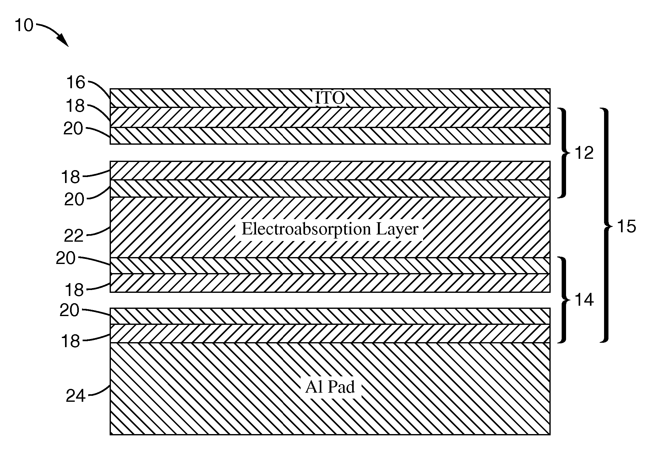
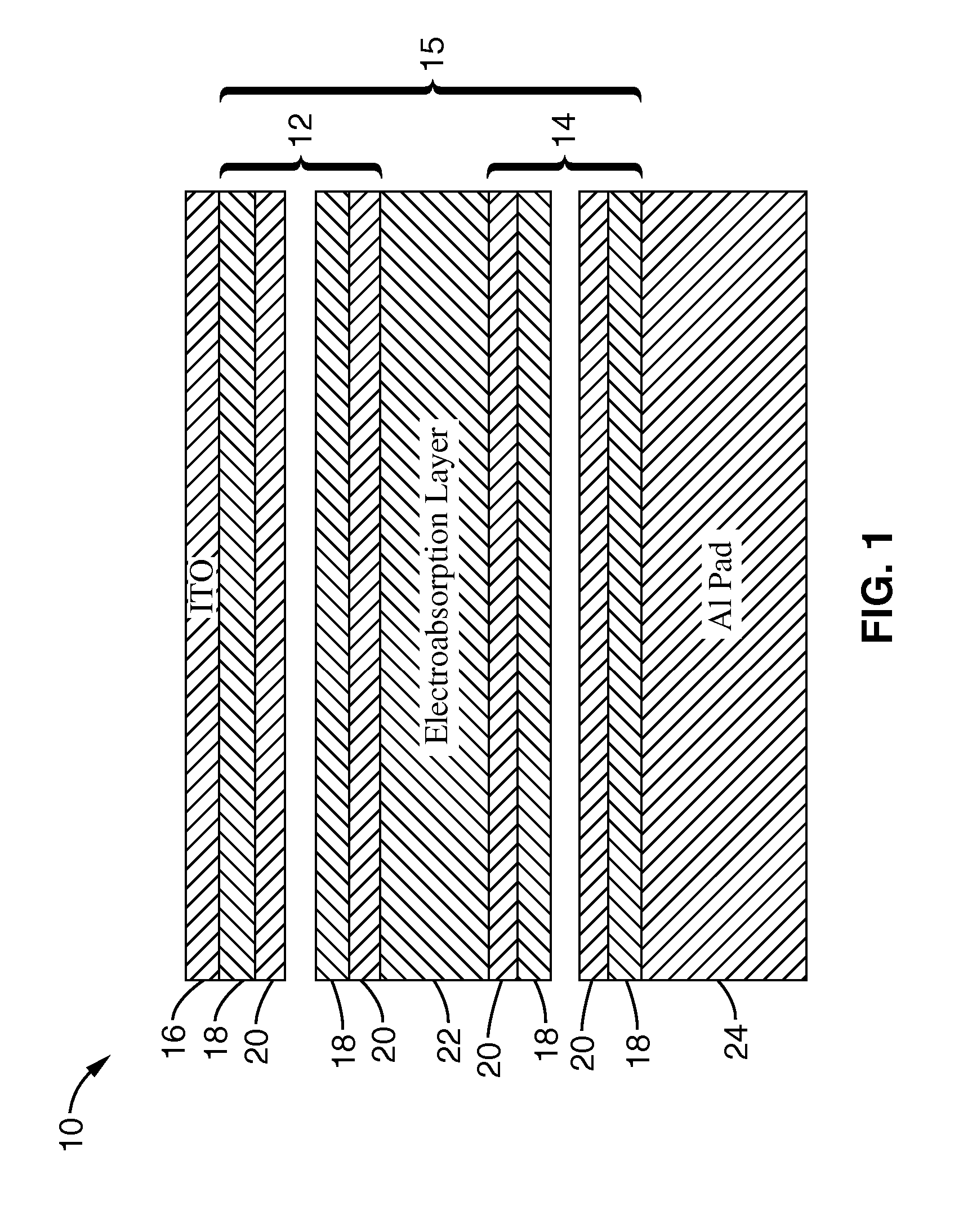
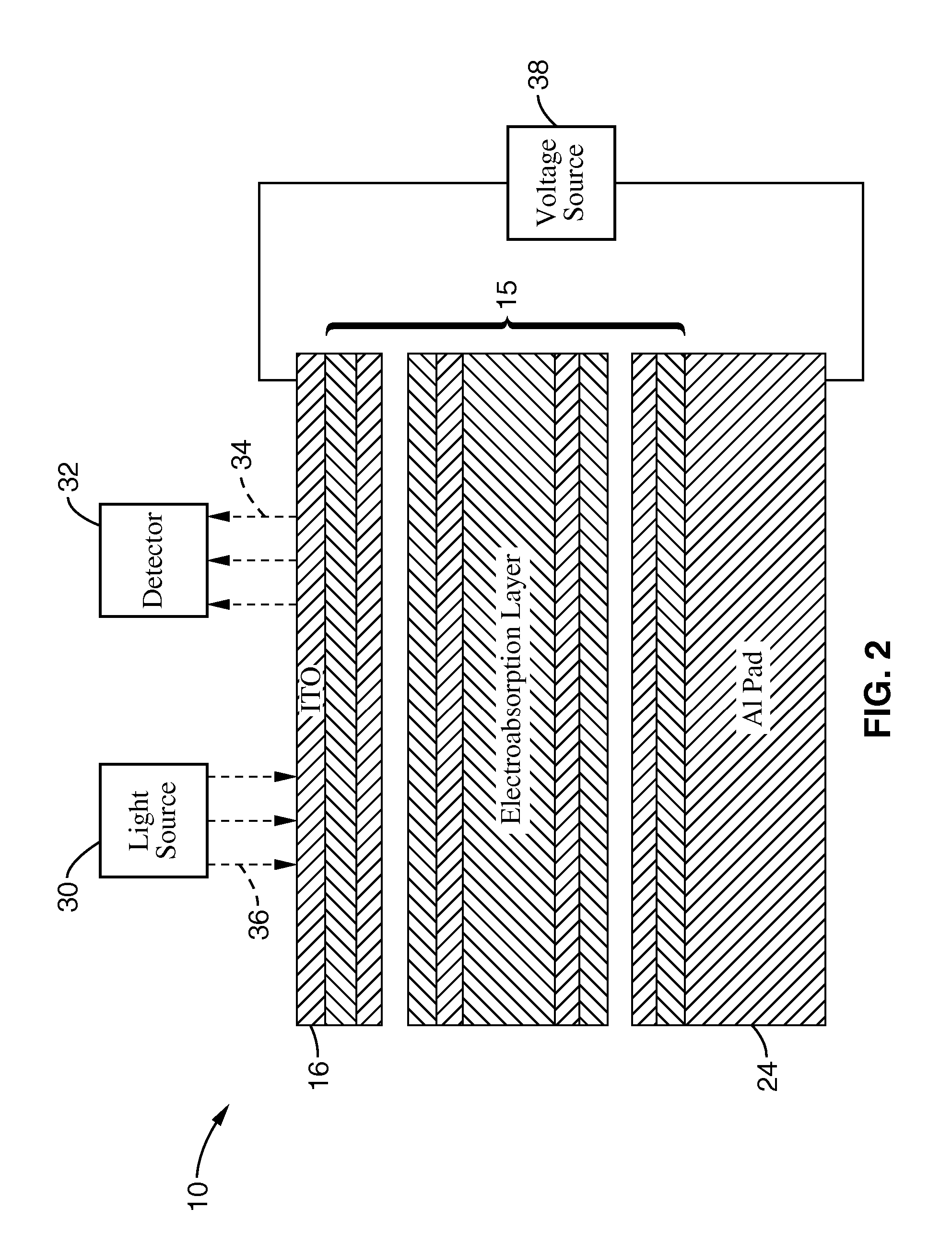
[0067] Referring more specifically to the drawings, for illustrative purposes the present invention is embodied in the apparatus generally shown in FIG. 1 through FIG. 3 and FIG. 4B through FIG. 10. It will be appreciated that the apparatus may vary as to configuration and as to details of the parts, and that the method may vary as to the specific steps and sequence, without departing from the basic concepts as disclosed herein.

[0068] The present invention comprises an optical modulator that is based on electric field control of the saturation absorption threshold of semiconductor quantum dots, Si photodetectors, and an integrated optical transceiver on Si substrates. A vertical resonant cavity is used for boosting the optical power from that of a commercially available semiconductor laser by 50-100 times to the saturation intensity of the quantum dots. The optical modulator of the present invention is based on a completely new operational principles.

[0069] The modulator of the pr...


PUM


Abstract

A modulator for an optical transceiver is disclosed. The modulator has two quarter-wave stack mirrors composed of alternating dielectric layers with an optically absorbing layer sandwiched in between to form the vertical resonant cavity. The optically absorbing layer is made of semiconductor nanocrystals embedded in a dialectic material. The device is configured to operate near the saturation point of the absorption layer. By adjusting the biasing voltage across the absorption layer, the saturation threshold of the semiconductor nanocrystals is altered, resulting in the overall reflectivity of the resonant cavity to vary. The modulator is configured to be fabricated as the extension of the backend process of Si CMOS.

Description

CROSS-REFERENCE TO RELATED APPLICATIONS [0001] This application claims priority from, and is a 35 U.S.C. § 111 (a) continuation of, co-pending PCT international application serial number PCT / US2006 / 014578, filed on Apr. 18, 2006, incorporated herein by reference in its entirety, which claims priority from U.S. provisional application Ser. No. 60 / 672,911 filed on Apr. 18, 2005, incorporated herein by reference in its entirety. [0002] This application is also related to PCT International Patent Publication No. WO2006 / 113725 A2, published Oct. 26, 2006, and No. WO2006 / 113725 A3, published Mar. 1, 2007, each of which is incorporated herein by reference in its entirety.STATEMENT REGARDING FEDERALLY SPONSORED RESEARCH OR DEVELOPMENT [0003] Not Applicable INCORPORATION-BY-REFERENCE OF MATERIAL SUBMITTED ON A COMPACT DISC [0004] Not Applicable NOTICE OF MATERIAL SUBJECT TO COPYRIGHT PROTECTION [0005] A portion of the material in this patent document is subject to copyright protection under ...

Claims


Application Information

Patent Timeline
IPC IPC(8): H01L21/00G02F1/03H04B10/00
CPCG02F1/218G02F2001/213G02F2001/0157G02F1/0157G02F1/213
Inventor XIE, YA-HONGSHI, BIN
Owner RGT UNIV OF CALIFORNIA
Learn More