Substratum with conductive film and process for producing the same
a technology of conductive film and substrate, which is applied in the direction of vacuum evaporation coating, thermoelectric devices, coatings, etc., can solve the problems of complex production process, irregular surface formation of crystallized film, leak current or dark spot, etc., and achieve excellent flatness and transparency, excellent flatness, and small surface irregularities.
- Summary
- Abstract
- Description
- Claims
- Application Information
AI Technical Summary
Benefits of technology
Problems solved by technology
Method used
Image
Examples
example 1
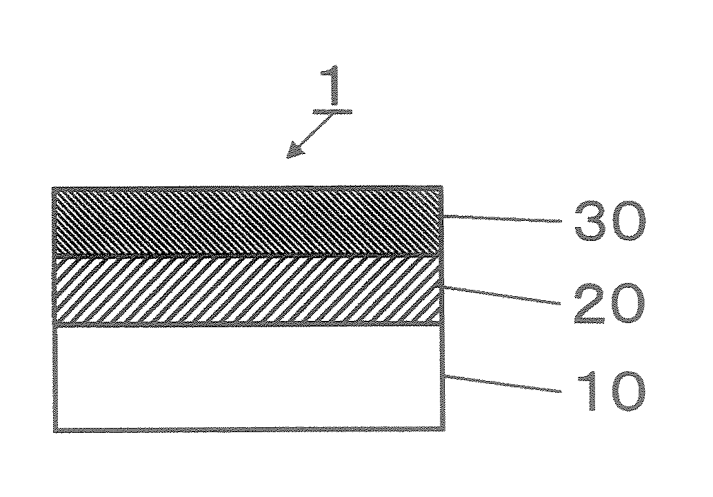
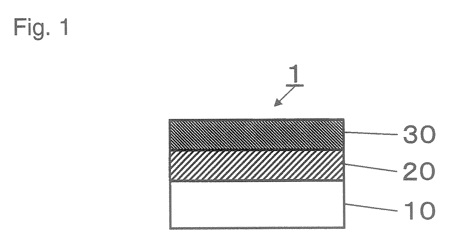
[0038] A cleaned soda lime silicate glass substrate (average surface roughness Ra was 0.5 nm, thickness was 0.7 mm, visible light transmittance was 85% ) was set in a sputtering apparatus, and heated to a substrate temperature of 250° C. On the substrate, a SiO2 film was formed as an alkali-barrier layer by an RF sputtering method using a SiO2 target. The flow rate ratio of Ar / O2 was 40 / 10, the pressure was 3 mTorr (0.4 Pa in SI unit) and the sputtering powder density was 2.74 W / cm2. The SiO2 film was formed to have film thickness of 20 nm. The composition of the film formed was the same as that of the target.
[0039] Then, on the SiO2 film, a Y2O3-doped ZrO2 film was formed as a foundation film by an RF sputtering method. The material of sputtering target used consisted of 3 mol % of Y2O3 (content of Y2O3 was 3 mol % based on total amount of Y2O3 and ZrO2 and 97 mol % of ZrO2. The flow rate ratio of ArO2 was 40 / 10, the pressure was 3 mTorr and the sputtering power density was 2.74 W...
example 2
[0042] A substrate with ITO film obtained in Example 1 was subjected to Ar ion etching using a linear ion source (manufactured by Advanced Energy: model LIS-38, irradiation area was 5 cm×38 cm). 30 sccm of Ar gas was flown in the linear ion source, and Ar gas was flown separately in a vacuum chamber to which the linear ion source was attached so that the pressure of entire system became 1.9 mTorr. The acceleration voltage of the linear ion source was set to 2 kV and the ion current was set to 210 mA. Under these conditions, the ITO film was irradiated with argon ion beam for 4 seconds (accumulated power was 0.0024 W·h).
[0043] The average surface roughness Ra of the ITO film after the ion etching treatment was measured, Ra was 0.9 nm.
example 3
[0044] The substrate with ITO film obtained in Example 1 was subjected to Ar ion etching by using a linear ion source (manufactured by Applied Ion Beam: model IS336, irradiation area was 5 cm×10 cm). 3 sccm of Ar gas was flown in the linear ion source so that the pressure in the entire chamber became 0.2 mTorr. The acceleration voltage of the linear ion source was set to 3 kV and the ion current was set to 45 mA. Under these conditions, the ITO film was Irradiated with argon ion beam for about 40 seconds (accumulated power was 0.005 W·h).
[0045] The average surface roughness Ra Of the ITO film after the ion etching treatment was measured. Ra was 0.6 nm.
PUM
| Property | Measurement | Unit |
|---|---|---|
| Thickness | aaaaa | aaaaa |
| Thickness | aaaaa | aaaaa |
| Surface roughness | aaaaa | aaaaa |
Abstract
Description
Claims
Application Information
 - R&D
- Intellectual Property
- Life Sciences
- Materials
- Tech Scout
- Unparalleled Data Quality
- Higher Quality Content
- 60% Fewer Hallucinations
Browse by: Latest US Patents, China's latest patents, Technical Efficacy Thesaurus, Application Domain, Technology Topic, Popular Technical Reports.
© 2025 PatSnap. All rights reserved.Legal|Privacy policy|Modern Slavery Act Transparency Statement|Sitemap|About US| Contact US: help@patsnap.com


