
Photoelectric Cells Utilizing Accumulation Barriers For Charge Transport

a photoelectric cell and charge transport technology, applied in the field of photovoltaic devices, can solve the problems of excess potential and charge accumulation on the absorber side of the interface, and achieve the effects of reducing the depletion potential, increasing temperature, and reducing the loss of internal field strength

Inactive Publication Date: 2007-10-04
WALSH KEVIN MICHAEL
View PDF10 Cites 9 Cited by
  • Summary
  • Abstract
  • Description
  • Claims
  • Application Information

AI Technical Summary

Benefits of technology

[0028] Another important advantage of the invention is that the built-in field is independent of temperature across a normal operating temperature range. This is because the Fermi levels in the WGS's are not expected to change due to their large energy band gaps and high carrier concentrations. Consequently the built-in field remains equal to the potential change across the full width of the a-Si:H band gap at all normal operating temperatures. Whereas in conventional solar cells the built-in field is dependant on carrier depletion within the absorber. The smaller band gap and lower carrier concentrations in the absorber means that the depletion potential is reduced with increasing temperature. This loss of internal field strength is the most important factor in the reduction in the power output of conventional cells with increasing temperature, usually quoted as a cell's (or module's) temperature coefficient.
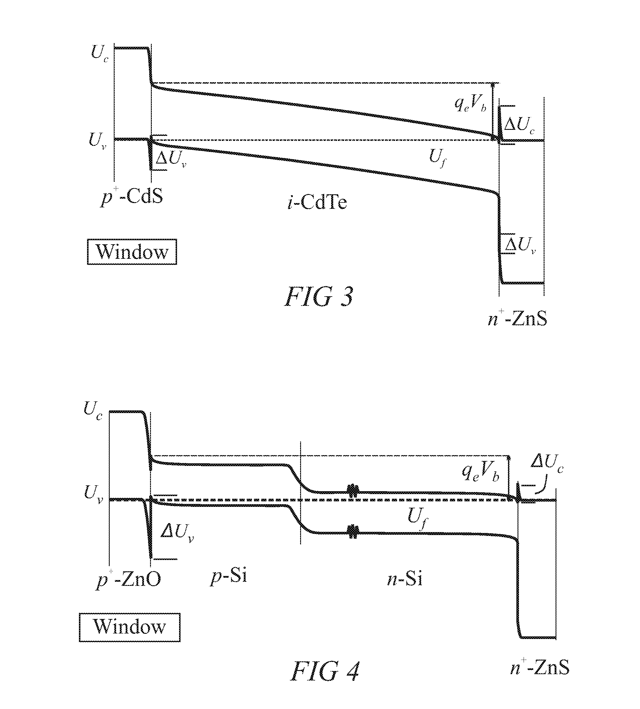
[0029]FIG. 3 illustrates, in the form of an equilibrium band diagram, the relevant sections of a P+-i-N+ solar cell that uses intrinsic CdTe as the active absorber. The cell makes use of p+-CdS and n+-ZnS as the contacts for hole and electron carrier collection, respectively. This junction has the same preferred features as illustrated in the a-Si:H cell, including carrier band offsets “ΔUv and ΔUc”, Fermi levels located within the WGS band edges and crossing through the band edges of i-CdTe at each interface. Most significantly, the cell of FIG. 3 should exhibit a larger built-in potential and lower recombination rates when compared to conventional CdTe cells, leading to an overall better photoelectric conversion efficiency.
[0030] The semiconductor arrangement illustrated in FIG. 3 is in contrast to prior art designs for CdTe solar cells, where conventionally p-CdTe is contacted at the front-side with n-CdS and at the rear with p-ZnTe (as described for example in U.S. Pat. No. 5,909,632 to Gessert). These contact semiconductors are preferred in convention designs due to the minimal carrier band offsets with CdTe at the contact interfaces. An additional distinguishing feature of conventional CdTe cells is the change in carrier type at the front contact from p-CdTe to n-CdS. Conversely, the invention's preferred arrangement is for an all-intrinsic absorber, where there is no change in carrier type at the interface. EXAMPLE 3 Crystalline Silicon Absorber
[0031]FIG. 4 is an equilibrium band diagram illustration of the relevant sections of a solar cell using lightly doped, crystalline silicon as the active absorber. The cell uses p+-ZnO (U.S. Pat. No. 6,908,782 “High carrier concentration p-type transparent conducting oxide films”) and n+-ZnS WGS contacts as the hole and electron carrier collectors, respectively. This junction again incorporates carrier band offsets “ΔUv and ΔUc” at each contact interface and may be symbolized as “P+-p-n-N+”. In contrast to the examples given above, the active absorber contains regions where the equilibrium carrier concentrations are both depleted (across the Si p-n junction) and accumulated (at the two contacts). In solar cell applications, crystalline silicon is typically made at least 50 microns thick to give near complete absorption of sunlight. Because of this, the total silicon thickness is not shown to scale in the figure in an attempt to better illustrate the features of the novel front and rear contacts.
[0032] This cell construction is similar to conventional crystalline cells with the exception of the contacts. It is notable that the total built-in potential across the silicon is equal to the silicon band gap and this potential drop is shared between both the depleted and accumulated regions. Whereas in a conventional silicon cell the built-in potential is limited to that created by the p-n depletion zone. Silicon solar cells also conventionally exhibit a rather large reduction in output with increasing temperature and this is believed to be primarily due to a reduction of the built-in potential across the p-n junction. It is anticipated that as the temperature of the cell shown in FIG. 4 rises, the total built-in potential will remain constant. An increasing proportion of the built-in potential will shift into the accumulation regions in compensation for a corresponding loss of potential across the p-n depletion zone. Thus, the cell of FIG. 4 should prove to be more efficient at all temperatures when compared to a conventional design, and most particularly at elevated temperatures.
[0033] The principle and mode of operation of this invention have been described in its preferred embodiments. However, it should be noted that this invention may be practiced otherwise than as specifically illustrated and described without departing from its scope. Numerous alterations and modifications of the basic template outlined above are possible. Some of these possible variations are listed below.

Problems solved by technology

This excess potential means that there will be a barrier to carrier transport across the interface for charge originating from within the absorber.
However, the excess potential also produces charge accumulation on the absorber side of the interface.

Method used


Image

  • Photoelectric Cells Utilizing Accumulation Barriers For Charge Transport
  • Photoelectric Cells Utilizing Accumulation Barriers For Charge Transport
  • Photoelectric Cells Utilizing Accumulation Barriers For Charge Transport

Examples


example 1

Amorphous Silicon Hydride (a-Si:H) Absorber

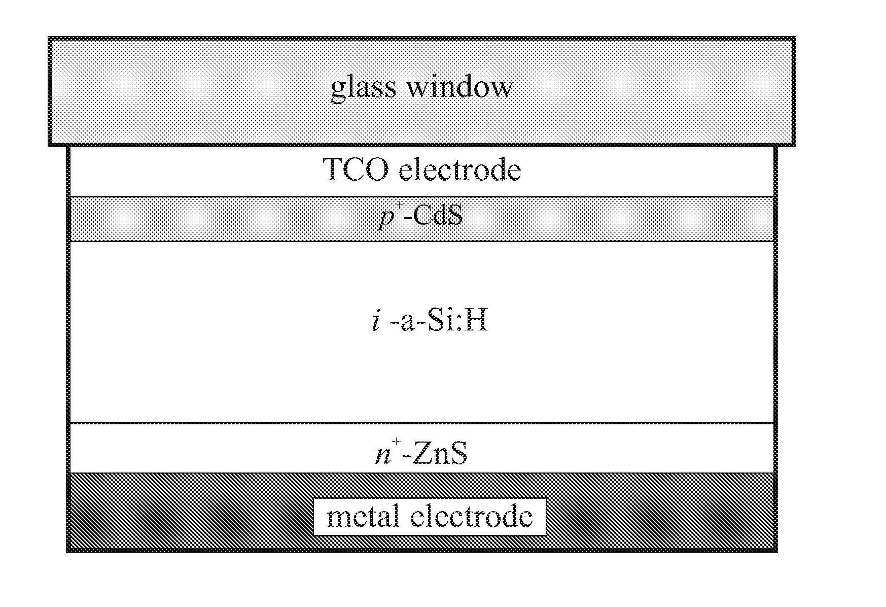
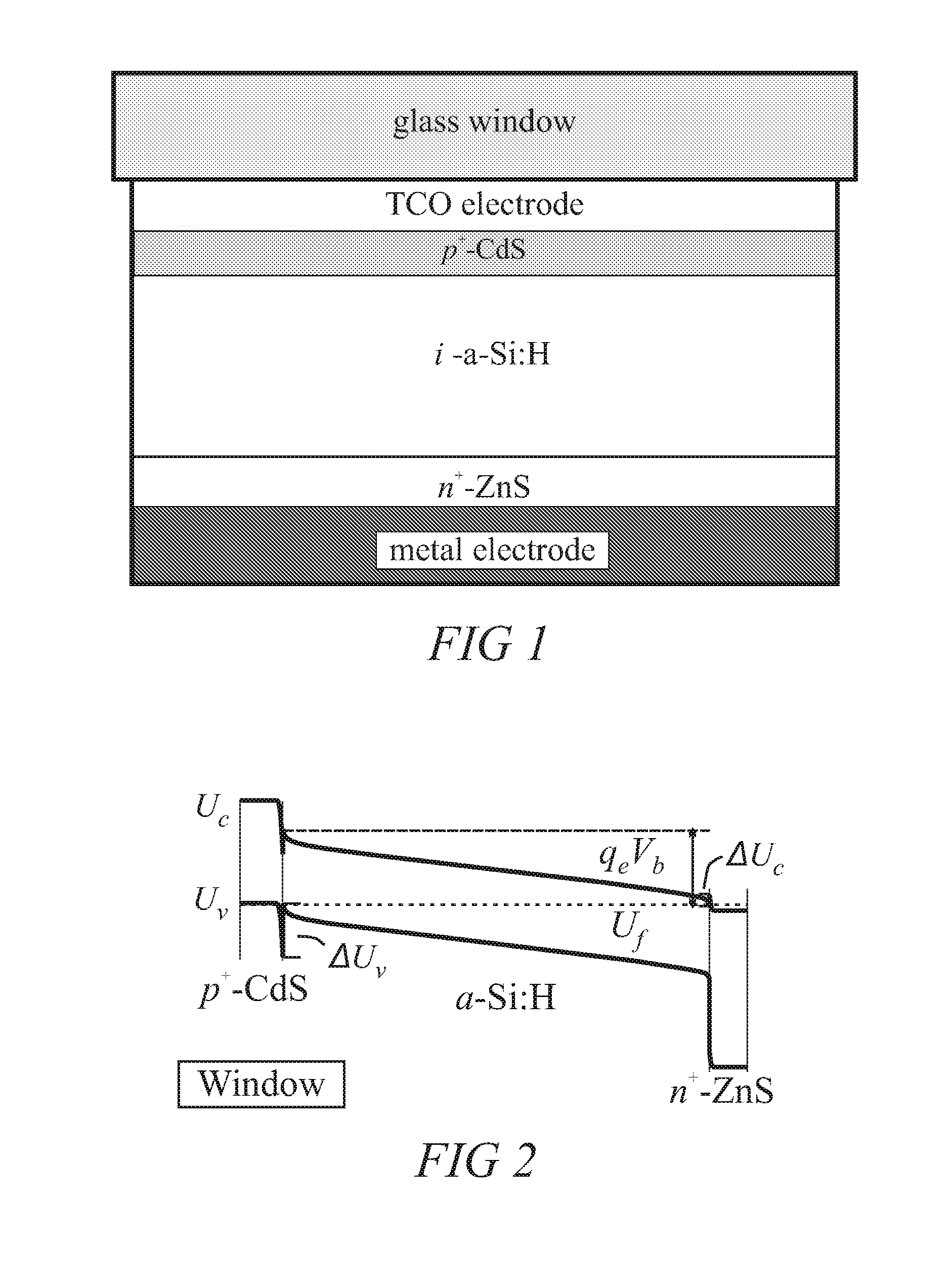
[0022] A schematic representation of one embodiment of the invention in which the absorber is amorphous silicon is shown in FIG. 1. The cell's photoactive region may be described as a modified p-i-n junction. A p-i-n (or n-i-p) junction consists of an extended junction, formed by placing an intrinsic (i) semiconductor layer between p- and n-layers of the same or similar semiconductors. The potential drop across the intrinsic layer is equal to the difference between the work function in the p- and n-layers. In the ideal case, the intrinsic layer contains relatively little space charge. Where this is true, the electric field strength is nearly uniform through the bulk absorber layer and varies inversely with the thickness of the i-layer. The p-i-n junction is usually found in solar cells in which the absorber is a-Si:H.

[0023] The modified p-i-n cell illustrated in FIG. 1 uses intrinsic a-Si:H (i-a-Si:H) as the active absorber. The i-a-Si:H ...

example 2

Cadmium Telluride (CdTe) Absorber

[0029]FIG. 3 illustrates, in the form of an equilibrium band diagram, the relevant sections of a P+-i-N+ solar cell that uses intrinsic CdTe as the active absorber. The cell makes use of p+-CdS and n+-ZnS as the contacts for hole and electron carrier collection, respectively. This junction has the same preferred features as illustrated in the a-Si:H cell, including carrier band offsets “ΔUv and ΔUc”, Fermi levels located within the WGS band edges and crossing through the band edges of i-CdTe at each interface. Most significantly, the cell of FIG. 3 should exhibit a larger built-in potential and lower recombination rates when compared to conventional CdTe cells, leading to an overall better photoelectric conversion efficiency.

[0030] The semiconductor arrangement illustrated in FIG. 3 is in contrast to prior art designs for CdTe solar cells, where conventionally p-CdTe is contacted at the front-side with n-CdS and at the rear with p-ZnTe (as describe...

example 3

Crystalline Silicon Absorber

[0031]FIG. 4 is an equilibrium band diagram illustration of the relevant sections of a solar cell using lightly doped, crystalline silicon as the active absorber. The cell uses p+-ZnO (U.S. Pat. No. 6,908,782 “High carrier concentration p-type transparent conducting oxide films”) and n+-ZnS WGS contacts as the hole and electron carrier collectors, respectively. This junction again incorporates carrier band offsets “ΔUv and ΔUc” at each contact interface and may be symbolized as “P+-p-n-N+”. In contrast to the examples given above, the active absorber contains regions where the equilibrium carrier concentrations are both depleted (across the Si p-n junction) and accumulated (at the two contacts). In solar cell applications, crystalline silicon is typically made at least 50 microns thick to give near complete absorption of sunlight. Because of this, the total silicon thickness is not shown to scale in the figure in an attempt to better illustrate the featu...


PUM


Abstract

The invention describes a means for electrically contacting the active semiconductor in a solar cell through the use of an accumulation barrier. A heavily-doped, wide-gap semiconductor serves as the contacting material. The carrier band of the contact lies at a substantially higher potential energy than that of the corresponding band of the absorber and an accumulation barrier at the contact interface is thus produced. This type of contact presents several advantages, including the ability to use an all-intrinsic absorber, the formation of a low resistance ohmic contact and providing for a large, temperature independent built-in potential across the absorber.

Description

CROSS-REFERENCE TO RELATED APPLICATIONS [0001] The application claims priority to U.S. Provisional Application Ser. No. 60 / 788,285 entitled “P-i-N tunneling Junction Photovoltaic Cell,” filed on Mar. 31, 2006.BACKGROUND OF THE INVENTION [0002] 1. Field of the Invention [0003] The present invention relates to a photovoltaic devices composed of semiconductors as the active light absorbing materials, and more particularly to a photovoltaic devices in which a means for contacting the active absorbers is provided that results in high photoelectric conversion efficiencies. [0004] 2. Related Background Art [0005] The operation of most photovoltaic cells is dependant upon the existence of a electric field (i.e. a built-in field that is present under dark, equilibrium conditions) within an active, light-absorbing semiconductor. The field is created by providing for a material that has an excess of mobile electrons at a relatively high potential energy in contact with a second material having...

Claims


Application Information

Patent Timeline
Patent Type & Authority Applications(United States)
IPC IPC(8): H01L31/00
CPCH01L31/075Y02E10/548H01L31/077Y02E10/546
Inventor WALSH, KEVIN MICHAEL
Owner WALSH KEVIN MICHAEL
Learn More