Method of cleaning semiconductor substrate conductive layer surface

Inactive Publication Date: 2007-05-17
TOKYO ELECTRON LTD
View PDF9 Cites 6 Cited by
  • Summary
  • Abstract
  • Description
  • Claims
  • Application Information

AI Technical Summary

Benefits of technology

[0007] It is, therefore, an object of the present invention to provide a method for cleaning a surface of a semiconductor substrate capable of sufficiently removing residual organic material and / or natural oxide, thereby preventing a damage on a side wall insulting film of a via hole, and preventing an adverse effect on the dielectric constant (k value).
[0009] Since the oxide film can be removed by cleaning a surface of a conductive layer by generating plasma containing hydrogen in the reaction chamber such that the surface of the conductive layer is cleaned by being reduced therewith, the cleaning can be performed without increasing the electric resistance and the dielectric constant (k value).

Problems solved by technology

Further, a native oxide film is inevitably formed on the surface of the conductive layer.
Such residual organic material or oxide causes a problem in that it causes an electric resistance of a vie hole portion to increase.
In this method, although the residual organic material is decomposed to be removed by injecting argon ions, since injecting the argon ions does not involve an ashing, residual organic material cannot be removed completely.
Hence, the surface cannot be cleaned sufficiently.
Further, native oxide cannot be removed.
In addition, a damage is inflicted on an insulating film on a side wall of the via hole when the argon ions are injected, thus causing an adverse effect on the dielectric constant (k value).

Method used


Image

  • Method of cleaning semiconductor substrate conductive layer surface
  • Method of cleaning semiconductor substrate conductive layer surface
  • Method of cleaning semiconductor substrate conductive layer surface

Examples


Embodiment Construction

[0028] Hereinafter, a preferred embodiment in accordance with the present invention will be described with reference to accompanying drawings.

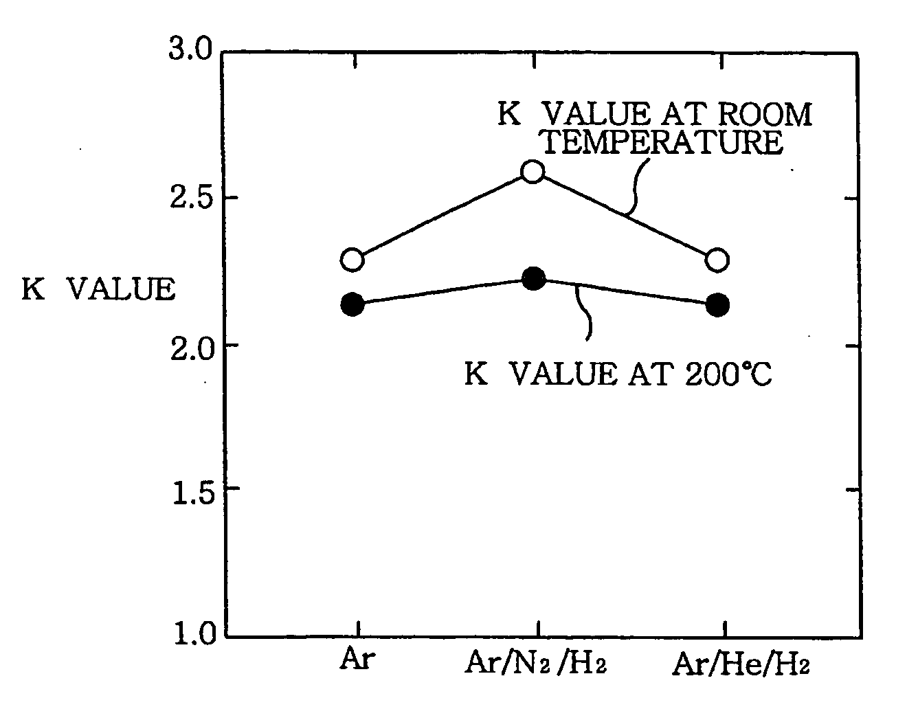
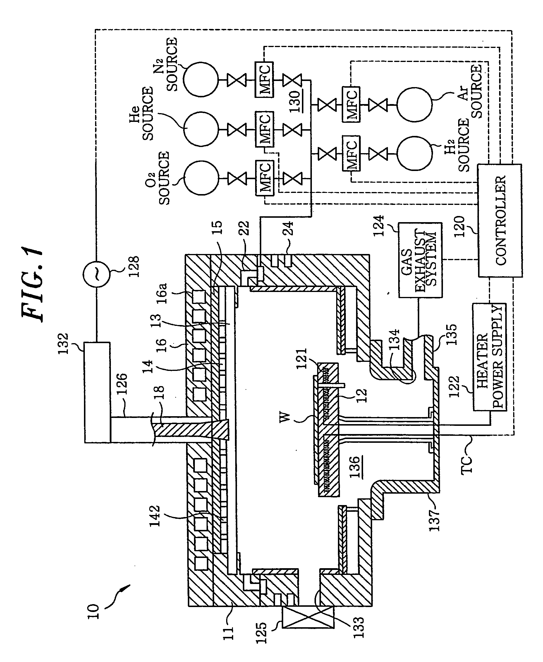
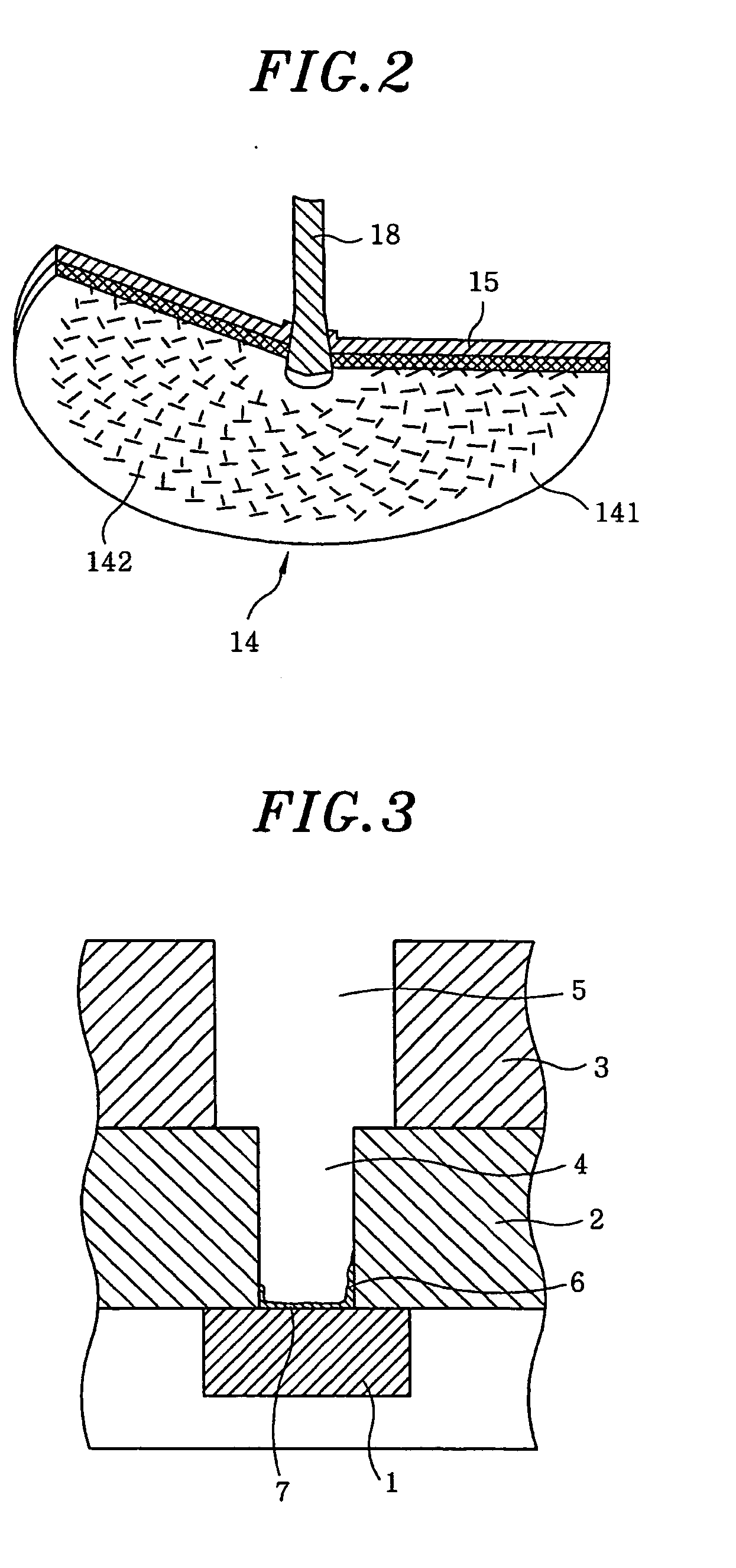
[0029]FIG. 1 shows a cross sectional view of a high density plasma processing apparatus 10 used for cleaning a dual damascene structure. FIG. 2 illustrates a partial cutaway perspective view of a slot plate installed in the high density plasma processing apparatus shown in FIG. 1.

[0030] The high density plasma processing apparatus 10 includes a processing chamber 11 having a substrate support 12 for supporting a semiconductor wafer W of a dual damascene structure. Gas in the processing chamber 11 is exhausted from an exhaust pipe 135 to a gas exhaust system 124 via a gas exhaust opening 136, an exhaust chamber 137 and an exhaust pipe opening 134. Further, the substrate support 12 includes a heater 121 for heating the semiconductor wafer W. The heater 121 is driven by an external heater power supply 122.

[0031] At an upper portion of the proc...


PUM


Abstract

A method of cleaning a semiconductor substrate conductive layer surface that can remove a residual organic material and a natural oxide satisfactorily and does not adversely affect a k value without damaging the side-wall insulation film of a via hole. A semiconductor device, including insulation films formed on the surface of a conductive layer of a semiconductor substrate and a via hole formed in an insulation film to partly expose the conductive layer, is carried into a reaction vessel, plasma including hydrogen is generated in the reaction vessel to clean the surface of the conductive layer at the bottom of the via hole, a residual organic material is decomposed and removed by ashing, and a copper oxide film on the surface of the conductive layer is reduced to Cu.

Description

FIELD OF THE INVENTION [0001] The present invention relates to a method for cleaning a surface of a conductive layer on a semiconductor substrate; and, more particularly, to a method for cleaning a surface of a conductive layer exposed through a bottom portion of a via hole in a dual damascene structure in which a wiring contact hole and a via hole are formed simultaneously. BACKGROUND OF THE INVENTION [0002] Conventionally, in a semiconductor device, there has been used a method for depositing and planarizing an interlayer insulating film after a wiring has been formed. As an idea different from this, there is a dual damascene structure in which a wiring trench and a via hole are formed simultaneously. In this structure, since the via hole can be formed of a same material as that of the wiring trench, an interface resistance of a contact hole can be reduced, and an electro-migration tolerance can be enhanced. Especially, in the dual damascene structure, hitherto demands for enhanci...

Claims


Application Information

Patent Timeline
IPC IPC(8): H01L21/4763H01L21/302H01L21/306H01L21/311H01L21/768
CPCH01J2237/335H01L21/02063H01L21/76838H01L21/76814H01L21/02068H01L21/3065
Inventor SASAKI, MASARUIDE, SHINJIOZAKI, SHIGENORI
Owner TOKYO ELECTRON LTD
Why Eureka
Try Eureka