
Process kit design to reduce particle generation

Inactive Publication Date: 2006-12-28
APPLIED MATERIALS INC
View PDF27 Cites 221 Cited by
  • Summary
  • Abstract
  • Description
  • Claims
  • Application Information

AI Technical Summary

Benefits of technology

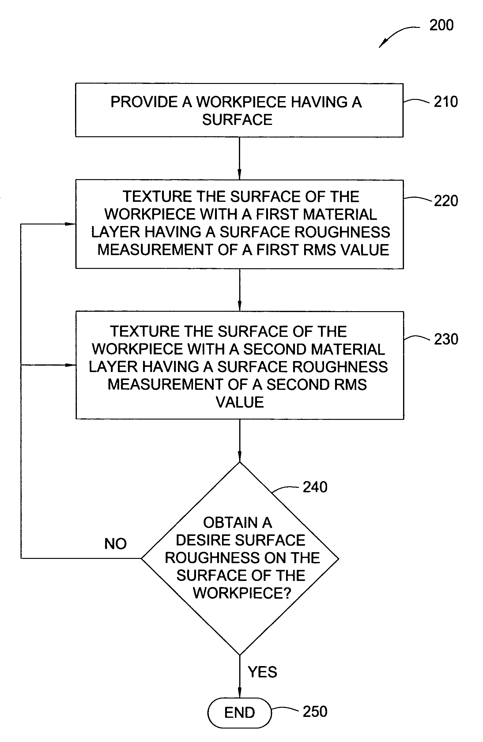
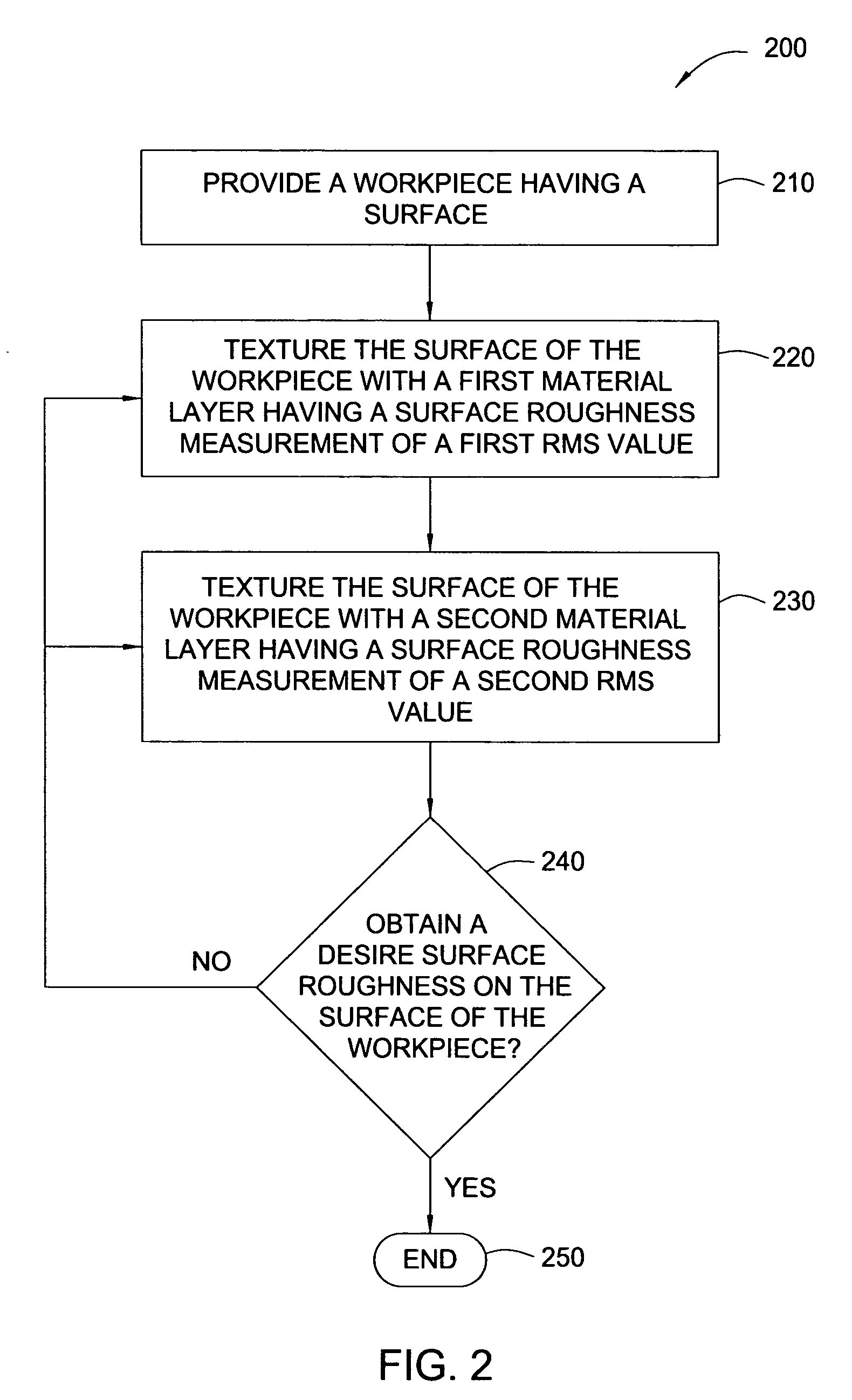
[0012] The present invention generally provides a method of providing a very rough texture to a surface of a work-piece. In one embodiment, the method includes coating one or more surfaces of one or more components of the process chamber with a first material layer having a surface roughness measurement of a first dimensional root mean square (RMS) of about 1200 micro-inches or less and arc spraying the surface of the first material layer with a second material layer having a surface roughness measurement of a second RMS of about 1500 micro-inches or more to roughen the surface of the one or more components.
[0014] In still another embodiment, a method of texturing a surface of a component for use in a semiconductor process chamber is provided. The method includes coating the surface of the component with a first material layer having a surface roughness measurement of a first RMS of about 1200 micro-inches or less and arc spraying the surface of the first material layer with a second material layer having a surface roughness measurement of a second RMS to roughen the surface of the component, the second RMS being larger than the first RMS.
[0015] Also provided is a method of reducing contamination in a process chamber. The method includes coating the surface of the component with a protective layer having a surface roughness measurement of a first RMS and arc spraying the surface of the protective layer with a material layer having a surface roughness measurement of a second RMS. The material layer may include the same material as the material of the component and the second RMS may be larger than the first RMS.

Problems solved by technology

As electronic devices and integrated circuit devices continue to be fabricated with reduced dimensions, the manufacture of these devices becomes more susceptible to reduced yields due to contamination.
Contamination of these devices may arise from sources including undesirable stray particles impinging on a substrate during thin film deposition, etching or other semiconductor wafer or glass substrate fabrication processes.
These condensed foreign particles or contaminants accumulating on the internal surfaces of the process chamber are prone to detaching or flaking off onto the surface of the substrate in between or during a substrate processing sequence.
These detached foreign particles may then impinge upon and contaminate the substrate and devices thereon.
Contaminated devices frequently must be discarded, thereby decreasing the manufacturing yield of the substrate processing.
The contamination problem is much more severe when a large area substrate is being processed.
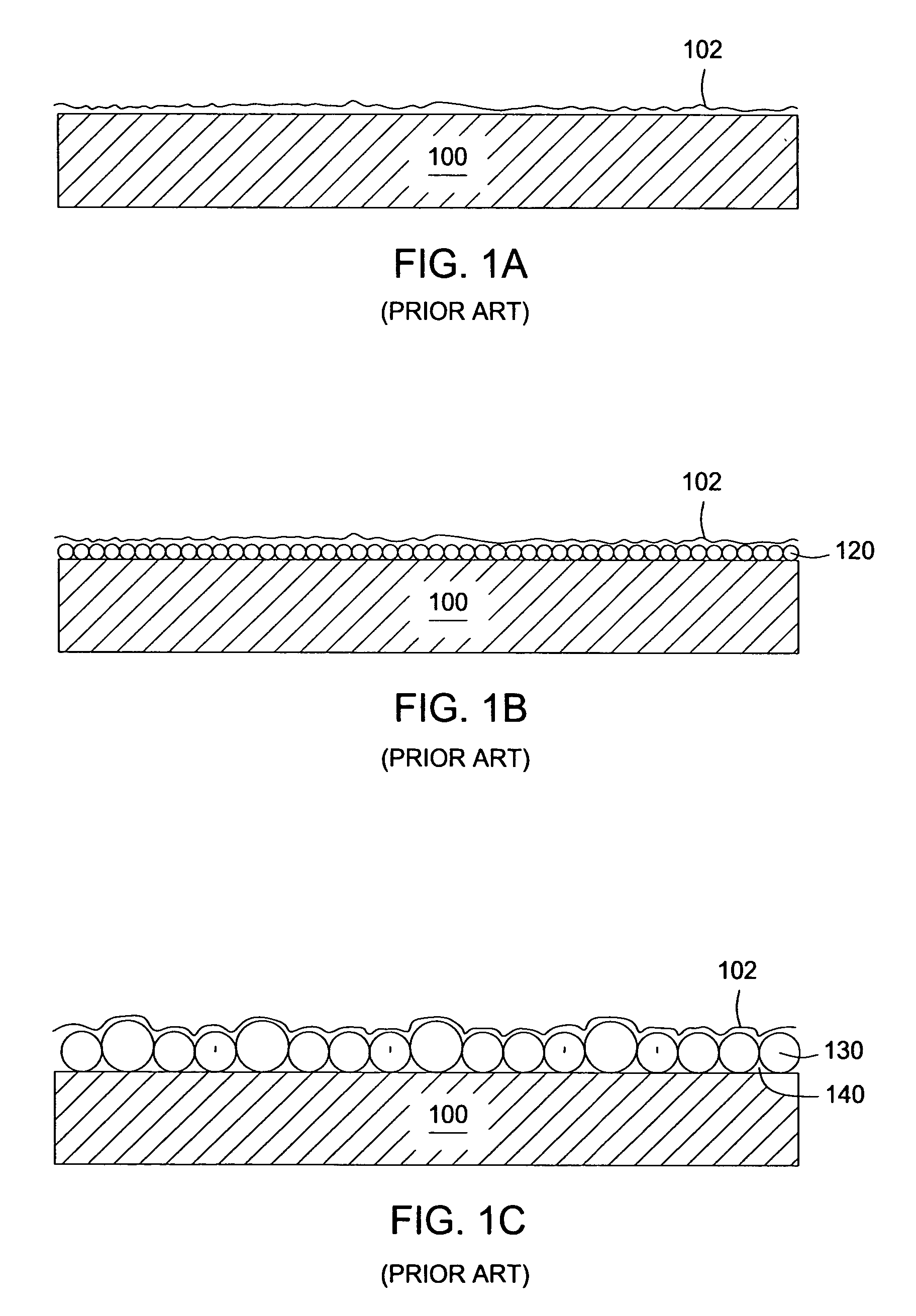
Thus, the textured surface coating 130 does not adhere strong enough to the surface of the work-piece 100 and a thick textured coating is not suitable due to its intrinsic high internal stress.
However, the bonding strength is typically low and internal surfaces of the process chamber need to be re-blasting or re-textured after only a few times of substrate processing.
Arc spray typically involves striking a DC electric arc between two continuous, thin consumable metal wire electrodes to form spray materials which are atomized by a jet of compressed gas into fine droplets and propelled onto a substrate surface, resulting in a low cost and high deposition rate spraying process.
However, these and other methods for providing textured internal surfaces within a process chamber are sometimes ineffective at creating sufficient adhesion or bonding between the condensed masses and the chamber internal surface.
Also, despite the amount of cleaning that is performed, in some instances contamination of delaminated, condensed materials onto the substrate during substrate processing in a process chamber may still occur.
Further, when various chamber parts and chamber walls are made from aluminum, aluminum arc spray may not be suitable since the texturing material and the chamber material are the same, and cleaning and re-texturing the internal surfaces of the process chamber will affect the integrity and thickness of the chamber components.

Method used


Image

  • Process kit design to reduce particle generation
  • Process kit design to reduce particle generation
  • Process kit design to reduce particle generation

Examples


Embodiment Construction

[0032] The present invention provides a method of providing a very rough-textured surface to a work-piece. A well-textured surface reduces the possibility of condensed materials flaking from the work-piece. For example, the work-piece may include various internal components / parts of a process chamber or a process kit such that rough internal surfaces of the process chamber can be used to attract and adhere various particles, condensed materials, contaminants generated during substrate processing. The invention further provides the process chamber and various chamber components having rough textured surfaces.

[0033]FIG. 2 illustrates a flow chart of a method 200 according to one embodiment of the invention to provide a very rough texture to a surface of a work-piece. At step 210, the work-piece having a surface is provided. The work-piece generally includes a material, such as a metal or metal alloy, a ceramic material, a polymer material, a composite material, or combinations thereo...


PUM

PropertyMeasurementUnit
Surface roughnessaaaaaaaaaa

Abstract

A method for making a process kit and a process kit design which has reduced particle generation during substrate processing are provided. The internal surface of the process kit design are textured by coating its surface with a first material layer having a smaller RMS surface roughness measurement and arc spraying with a second material layer or additional material layers having a larger RMS value. The first material layer can be coated by bead blasting, plating, arc spraying, thermal spraying, or other processes. In addition, the invention also provides selective coating of internal surface of the process kit with a protective layer and arc spraying the surface pf the protective layer with another material layer, which may be of the same material as the material of the internal surface of the process kit.

Description

BACKGROUND OF THE INVENTION [0001] 1. Field of the Invention [0002] Embodiments of the present invention generally relate to a method to modify the surface of a material part used in a process chamber. More particularly, embodiments of the present invention relate to modifying the surface of chamber components used in a process chamber to provide a textured surface thereon. [0003] 2. Description of the Related Art [0004] As electronic devices and integrated circuit devices continue to be fabricated with reduced dimensions, the manufacture of these devices becomes more susceptible to reduced yields due to contamination. Particularly, fabricating those devices having smaller device sizes requires the control of contamination to a greater extent than previously considered to be necessary. [0005] Contamination of these devices may arise from sources including undesirable stray particles impinging on a substrate during thin film deposition, etching or other semiconductor wafer or glass s...

Claims


Application Information

Patent Timeline
IPC IPC(8): B05D1/08C23C16/00
CPCC23C14/042C23C14/564C23C16/4581C23C16/4404C23C16/042
Inventor LE, HIEN-MINH HUUINAGAWA, MAKOTO
Owner APPLIED MATERIALS INC
Learn More