Transparent electroconductive substrate, dye-sensitized solar cell electrode, and dye-sensitized solar cell

Inactive Publication Date: 2006-10-19
BRIDGESTONE CORP
View PDF2 Cites 28 Cited by
  • Summary
  • Abstract
  • Description
  • Claims
  • Application Information

AI Technical Summary

Benefits of technology

[0011] A dye-sensitized solar cell electrode according to the second aspect includes the transparent electroconductive substrate of the first aspect and a dye-adsorbed semiconductor layer formed on the ITO layer of the transparent electroconductive substrate. By using a polymer film as the base, the dye-sensitized solar cell electrode can be flexible.
[0012] The acid-resistant transparent electroconductive substrate of the first aspect is highly resistant to acids and significantly useful for applications requiring acid resistance. The acid-resistant transparent electroconductive substrate used in the second aspect is advantageous in preparing a dye-sensitized semiconductor electrode for a dye-sensitized solar cell by forming a layer-by-layer self-assembled film on the ITO layer by a layer-by-layer assembly technique, forming a replica layer by acid-treating the layer-by-layer self-assembled film to form irregularities, and forming a semiconductor layer on the replica layer.
[0017] The dye-sensitized solar cell electrode of the fifth aspect includes the transparent electroconductive substrate of the fourth aspect and a dye-adsorbed semiconductor layer formed on the titanium oxide thin layer of the transparent electroconductive substrate. By using a polymer film as the base, the dye-sensitized solar cell electrode can be flexible.
[0018] The acid-resistant transparent electroconductive substrate of the fourth aspect is superior in acid resistance and significantly useful for applications requiring acid resistance. The acid-resistant transparent electroconductive substrate used in the fifth aspect is advantageous in preparing a dye-sensitized semiconductor electrode for a dye-sensitized solar cell by forming a layer-by-layer self-assembled film on the transparent electroconductive layer, such as an ITO layer, by a layer-by-layer assembly technique, forming a replica layer by acid-treating the layer-by-layer self-assembled film to form irregularities, and forming a semiconductor layer on the replica layer.
[0020] Seventh to ninth aspects of the present invention are intended to provide a transparent electroconductive body useful for a dye-sensitized solar cell electrode. The transparent electroconductive body has a sufficiently low resistance, is not corroded by electrolytes, and is effective in increasing the photoelectric conversion efficiency of dye-sensitized solar cells. Seventh to ninth aspects are also intended to provide a dye-sensitized solar cell electrode including the transparent electroconductive body, and a dye-sensitized solar cell including the electrode.

Problems solved by technology

The sol-gel process requires that the substrate 1 has such a high heat resistance as glass has, and does not allow the use of, for example, thermally unstable polymer films.
This is why a flexible, lightweight and thin dye-sensitized solar cell is difficult to achieve.
Polymer films are thermally unstable, and accordingly it is unsuitable to form an FTO layer on the polymer films by CVD (chemical vapor deposition).
Therefore such a metal or alloy layer cannot be formed.
However, the resistances of metal oxide transparent electroconductive layers are not sufficiently low.
This is a cause of low photoelectric conversion efficiency of the dye-sensitized solar cell.

Method used


Image

  • Transparent electroconductive substrate, dye-sensitized solar cell electrode, and dye-sensitized solar cell
  • Transparent electroconductive substrate, dye-sensitized solar cell electrode, and dye-sensitized solar cell
  • Transparent electroconductive substrate, dye-sensitized solar cell electrode, and dye-sensitized solar cell

Examples


example 1

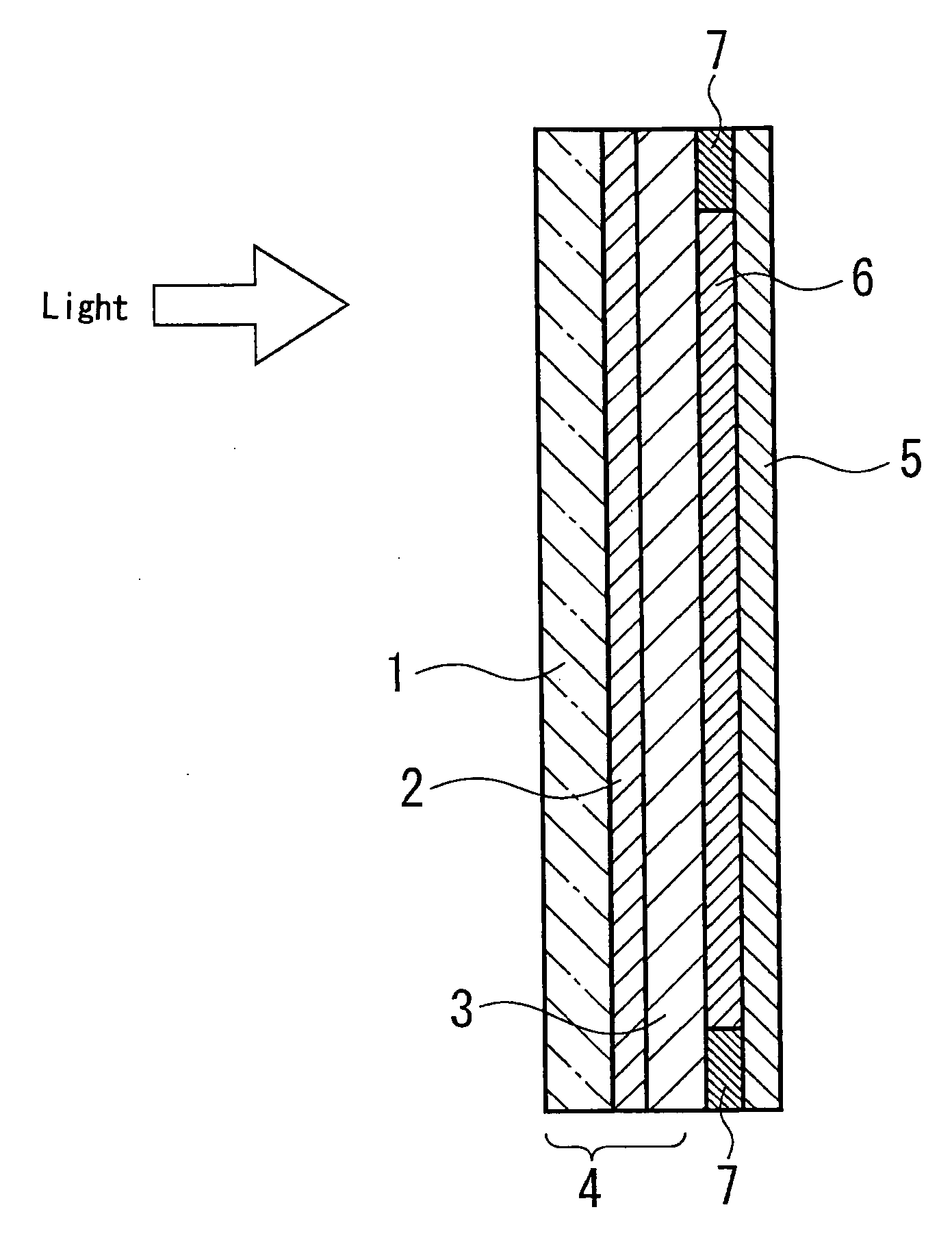
[0067] An ITO target (SnO2 content: 36 percent by weight) was set to a magnetron DC sputtering apparatus, and a 188 μm thick PET film was placed in a vacuum chamber. The vacuum chamber was evacuated to 5×10⁻⁴ Pa with a turbo molecular pump, and subsequently Ar gas and O2 gas were introduced as a gas mixture at flow rates of 197 sccm and 3 sccm respectively so as to adjust the pressure in the chamber to 0.5 Pa. Then, a power of 4 kW was applied to the ITO target, and thus an ITO layer, or transparent electroconductive film, was formed to a thickness of about 300 nm on the PET film.

[0068] The transparent electroconductive film was immersed in a hydrochloric acid aqueous solution with a pH of 2.0, and the surface resistance with time was measured to evaluate the acid resistance. The results are shown in Table 1.

example 2

[0087] An ITO target (SnO2 content: 10 percent by weight) and a Ti target were set to a magnetron DC sputtering apparatus, and a 188 μm thick PET film was placed in a vacuum chamber. The vacuum chamber was evacuated to 5×10⁻⁴ Pa with a turbo molecular pump, and subsequently Ar gas and O2 gas were introduced as a gas mixture at flow rates of 197 sccm and 3 sccm respectively so as to adjust the pressure in the chamber to 0.5 Pa. Then, a power of 4 kW was applied to the ITO target, and thus an ITO layer was formed to a thickness of about 300 nm on the PET film. Then, after completely purging the chamber with Ar gas, Ar gas and O2 gas as the gas mixture were introduced again to the chamber at flow rates of 170 sccm and 30 sccm respectively so as to adjust the pressure to 0.5 Pa. Then, a power of 6 kW was applied to the Ti target and a TiO2 thin layer was formed to a thickness of about 30 nm on the ITO layer by reactive sputtering, thus forming the transparent electroconductive film.

[00...


PUM

PropertyMeasurementUnit
Percent by massaaaaaaaaaa
Thicknessaaaaaaaaaa
Weightaaaaaaaaaa

Abstract

An acid-resistant transparent electroconductive substrate with an ITO layer includes a transparent base and the ITO layer formed over the transparent base. The ITO layer contains at least 30 percent by weight of tin oxide. A dye-sensitized solar cell electrode includes the transparent electroconductive substrate and a dye-adsorbed semiconductor layer formed over the ITO layer of the transparent electroconductive substrate. A dye-sensitized solar cell is provided which uses the dye-sensitized solar cell electrode as a dye-sensitized semiconductor electrode. A SnO2 content of 30 percent by weight or more enhances acid resistance. The dye-sensitized semiconductor electrode for the dye-sensitized solar cell is prepared by forming a layer-by-layer self-assembled film on the ITO layer by a layer-by-layer assembly technique, forming a replica layer by acid-treating the layer-by-layer self-assembled film to form irregularities, and forming a semiconductor layer on the replica layer.

Description

CROSS REFERENCE TO RELATED APPLICATION [0001] This is a continuation application of PCT / JP2004 / 15590 filed on Oct. 21, 2004.TECHNICAL FIELD [0002] The present invention relates to a transparent electroconductive substrate having such a high acid-resistance as is sufficient for applications requiring high acid resistance, and to a dye-sensitized solar cell electrode and a dye-sensitized solar cell that include the transparent electroconductive substrate. [0003] The present invention relates to a transparent electroconductive body suitable for a transparent electrode disposed on the lower side of a semiconductor electrode and for an opposing electrode that is opposed to a dye-sensitized semiconductor electrode with an electrolyte in between, to a dye-sensitized solar cell electrode using the transparent electroconductive body, and to a dye-sensitized solar cell including the dye-sensitized solar cell electrode as the opposing electrode. BACKGROUND OF THE INVENTION [0004] It has been k...

Claims


Application Information

Patent Timeline
IPC IPC(8): B32B17/06B32B9/00B32B19/00H01G9/20H01L31/0224H01M14/00
CPCC01G15/00C01G19/00C01G19/02C01P2002/52C01P2004/61C01P2004/62Y02E10/542H01G9/2031H01G9/2059H01L31/022466H01L2251/308H01M14/005C01P2006/40H01L31/022475H10K2102/103
Inventor OHNO, SHINGOIWABUCHI, YOSHINORIKOTSUBO, HIDEFUMIMORIMURA, YASUHIROSUGI, SHINICHIROSUGIYAMA, HIDEOYOSHIKAWA, MASATO
Owner BRIDGESTONE CORP
Why Eureka
Try Eureka