Surface improvement method in fabricating high temperature superconductor devices
a superconductor and surface improvement technology, applied in the manufacture/treatment of superconductor devices, superconductor devices, electric devices, etc., can solve the problems of affecting the growth of subsequent films or multi-layer films, and reducing the superconducting performance of single crystal substrates. , to achieve the effect of improving surface microstructure, improving surface microstructure, and high compactness
- Summary
- Abstract
- Description
- Claims
- Application Information
AI Technical Summary
Benefits of technology
Problems solved by technology
Method used
Image
Examples
embodiment 1
[0057] Ion surface modification with ion beam bombardment is conducted to a cold rolled Ni substrate.
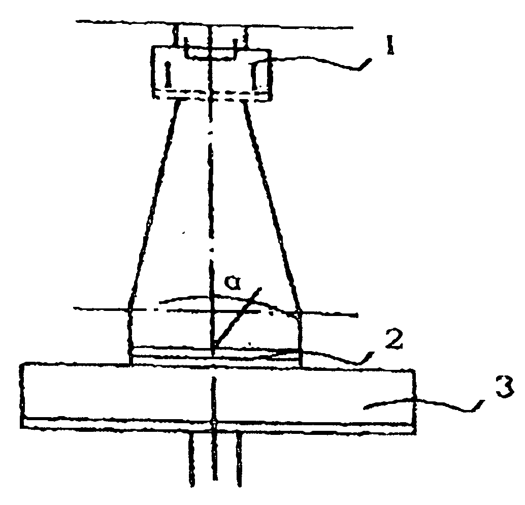
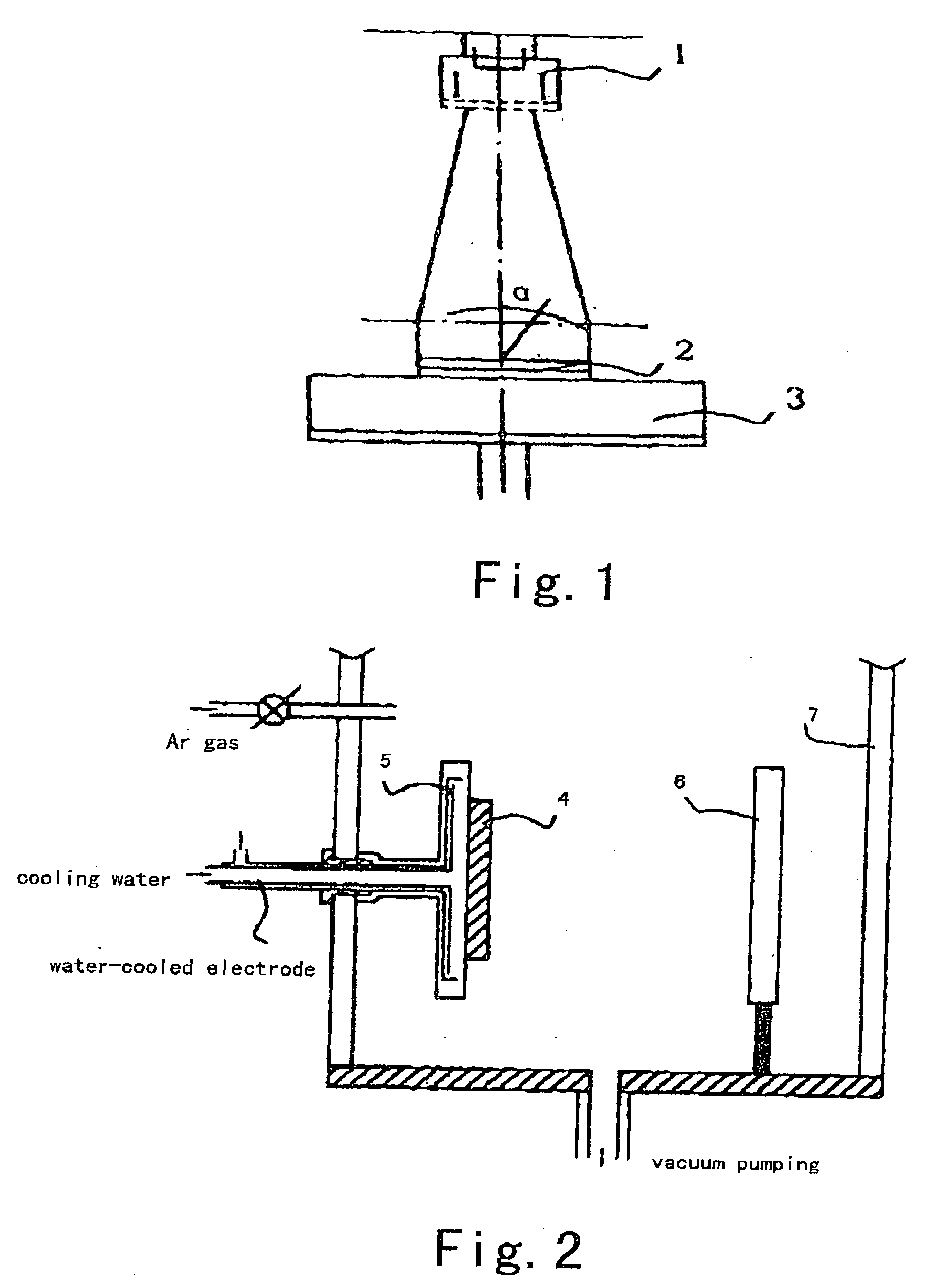
[0058]FIG. 1 shows a schematic diagram of reaction chamber structure, which includes a bombardment ion source 1, a sample 2, i.e., a clean rolled Ni substrate, and a sample support 3. The background air pressure of the reaction chamber is 6×10⁻⁴ Pa.
[0059] In experiment, the thickness of the cold rolled Ni substrate is 75-120 μm. The substrate is bombarded by Ar+ ion beam of 1200 eV, 60 mA, along different incidence angles. As a result, the biaxially textured Ni substrate with (100) preferred orientation is obtained by ion beam bombardment.
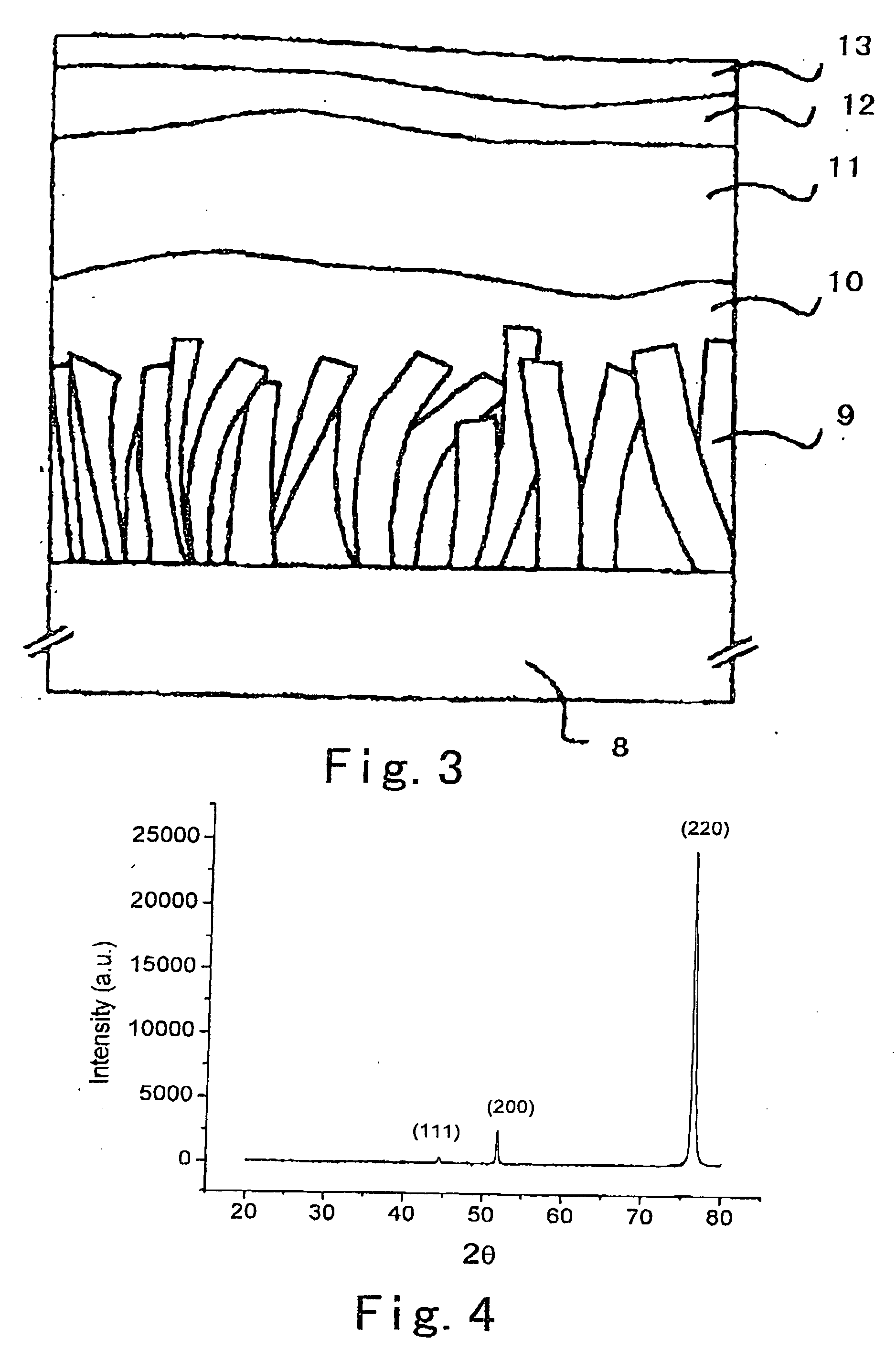
[0060]FIG. 4 is a typical x-ray θ-2θ diffraction curve of cold rolling Ni tape, and shows random orientation of crystalline grains, including not only a (200) diffraction peak, but also (111) and (220) diffraction peak.
[0061]FIG. 5 is an x-ray θ-2θ diffraction curve of Ni tape subjected to the ion beam bombardment along incidence angle of 45°, a...
embodiment 2
[0064] The ion surface modification is conducted to LaAlO3 film with plasma sputtering method.
[0065] On the clean Ni tape with biaxial texture, a LaAlO3 buffer layer film with biaxial texture is deposited and obtained through non-vacuum process. The resulting sample is put into the reaction chamber with high vacuum and is subjected to plasma sputtering. The structure of the reaction chamber is shown as FIG. 2, which includes a sample 4, a sample support 5, an electrode 6 and a wall of vacuum chamber 7. The background vacuum of the reaction chamber is 10−3-10−4 Pa. After the voltage of 400-600v is applied to two ends of the electrode, argon gas is filled and glow discharge occurs. The plasma input power is 75 W at 13.65 MHz and glowing time is 1 minute. YBCO film grows on the modified film of LaAlO3, and then is coated with a passivation layer and a protection layer. The resulting high temperature superconducting device conductor has a cross-section shown in FIG. 3, and comprises a ...
embodiment 3
[0066] Ion surface modification is conducted to YBCO film with ion beam bombardment.
[0067] The schematic structure of the reaction chamber is shown as FIG. 1, which includes a bombardment ion source 1, a sample 2, i.e., a clean YBCO film, and a sample support 3. The background air pressure of the reaction chamber is 6×10⁻⁴ Pa. The film is bombarded with Ar+ ion beam of 60 mA and 450 eV, along incidence angle of 5-85 degree. Mechanical scanning of ion beam on the platform is realized through synchronous swing of the system. The result shows that the ion beam sputtering improves surface smoothness and compactness of YBCO material, and reduces surface cracks.
[0068] Although only one particle beam is mentioned in this embodiment, two or more particle beams may be used, in the practical process, to bombard the material surface at the same time. For instance, in order to attain both the surface smoothness and biaxial texture of the processed material, the appropriate arrangement between...
PUM
 Abstract
Description
Claims
Application Information
 - R&D
- Intellectual Property
- Life Sciences
- Materials
- Tech Scout
- Unparalleled Data Quality
- Higher Quality Content
- 60% Fewer Hallucinations
Browse by: Latest US Patents, China's latest patents, Technical Efficacy Thesaurus, Application Domain, Technology Topic, Popular Technical Reports.
© 2025 PatSnap. All rights reserved.Legal|Privacy policy|Modern Slavery Act Transparency Statement|Sitemap|About US| Contact US: help@patsnap.com


