
Surface-coating method

Active Publication Date: 2006-06-29
COMMISSARIAT A LENERGIE ATOMIQUE ET AUX ENERGIES ALTERNATIVES
View PDF9 Cites 90 Cited by
  • Summary
  • Abstract
  • Description
  • Claims
  • Application Information

AI Technical Summary

Benefits of technology

[0063] One particularly important aspect of the invention is that very good adhesion of a material of interest chosen from one of these two categories is achieved by combining its deposition with that of a complementary material chosen from the other category.
[0203] In the case, for example, where it is difficult to find a liquid that is a good swelling agent for the first material and in which the precursors of the second material can also be dissolved, the third embodiment of the present invention will advantageously be used. Specifically, if no swelling agent is suitable, it is possible, according to the invention, to use a solvent that dissolves the precursors of the second material and that can also deposit the first material onto the surface. This third embodiment may be implemented, for example, using a solution containing both the first material, for example the layerable polymer, and the precursor of the second material, for example the reinforcing material. The deposition of the first material may be performed, for example, by centrifugation (“spin-coating”) or by any other suitable technique indicated in the present text. Once the deposit has been produced, a polymer film which already contains the precursors of the second material is obtained. Thus, according to this third embodiment, the step of inserting the precursor is performed simultaneously with the step of depositing the first material onto the surface of the substrate. This embodiment, which avoids an independent step of inserting the precursor of the second material into the first material and also possible washing of the surface before converting the precursor into the second material, allows time to be saved in the application of the process of the invention. The step of constructing the reinforcing material within the layerable material remains unchanged.

Problems solved by technology

These may especially be unstable functional groups, formed transiently, for instance radicals formed by vigorous oxidation of the surface, either chemically or via irradiation.
Unfortunately, these methods require relatively complex and expensive pretreatments, such as the use of vacuum installations for the plasma methods such as chemical vapour deposition (CVD), the technique of plasma-assisted chemical vapour deposition (PACVD), irradiation, etc., which, moreover, do not necessarily preserve the chemical integrity of the precursors.
However, these reactions cannot be exploited in all situations.
However, besides the fact that it is impossible to form an oxide layer on gold or on many noble metals, the solidity of the interface manufactured between the organic molecule of interest and the metal surface depends on the oxide layer.
This step requires a very low pH, and is therefore not compatible with all functional groups.
Furthermore, it is generally observed that the solutions prepared from aryl diazonium salts are unstable in the short term, especially due to the fact that these salts are heat- and photo-cleavable: this therefore limits their practical applicability.
Furthermore, this process does not make it possible, in practice, to produce thick layers, which leads to a relatively small number of grafted functional groups, which are very close to the surface.
However, since the process is based on the in situ synthesis of the polymer on the surface, major restrictions arise regarding the nature of the eligible precursor monomers, and thus of the types of polymers that may be deposited onto conductive or semiconductive surfaces via this process: It appears that only vinyl monomers and cyclic molecules that are cleavable by nucleophilic or electrophilic attack, for instance lactones, are compatible with these mechanisms, due to the fact that they are the only molecules that can polymerize via ionic chemical growth.
As a result of these restrictions, electrografting unfortunately cannot therefore offer a systematic solution for the attachment of any type of polymer material onto a surface.
In addition, even with these additives, this process constructs abrupt and thus weak interfaces, unless a high-temperature annealing operation is performed to bring about fusion at the interface.
Furthermore, the electrodeposition of metals onto semiconductive surfaces, especially when they are finely worked and when a deposit that marries the fine work is required, remains impossible, especially because the electrodeposition reaction is an electro-controlled reaction, and is therefore highly sensitive to the ohmic drop topology.
However, the interface constructed by CVD or by PVD between the copper of the seed layer and the semiconductor surface, known as the barrier layer, is abrupt.
The very low affinity of copper for these barrier materials gives rise to adhesion problems at the copper / barrier interface, especially at very low thicknesses (<50 nm).
These adhesion problems are sources of mechanical constraints at the time of annealing, of interface ruptures and thus of reduction in yield in the process.
These problems constitute, at the present time still, a concern and a major challenge for the success of the Damascene process, in particular at very fine etchings of 0.1 μm and below, and require complementary means to reinforce the interface between the seed layer and the semiconductive barrier materials.
By nature, these materials have an electronic structure that is very different from that of electrically conductive and semiconductive materials, so much so that it is difficult to envisage promoting bonds at the ionic insulator / conductor or ionic insulator / semiconductor interface.
The interface between these precipitated salts and electrically conductive or semiconductive surfaces thus remains abrupt and at the very least uncontrolled.
For the reasons of differences in electronic structures recalled above, the reinforcement of the interfaces between these solids and a conductive or semiconductive surface remains problematic, and the abovementioned drawbacks are not solved.

Method used


Image

  • Surface-coating method
  • Surface-coating method
  • Surface-coating method

Examples


example 1

Attachment of Copper to a Gold Surface by Armouring Using an Electrografted P4VP Film

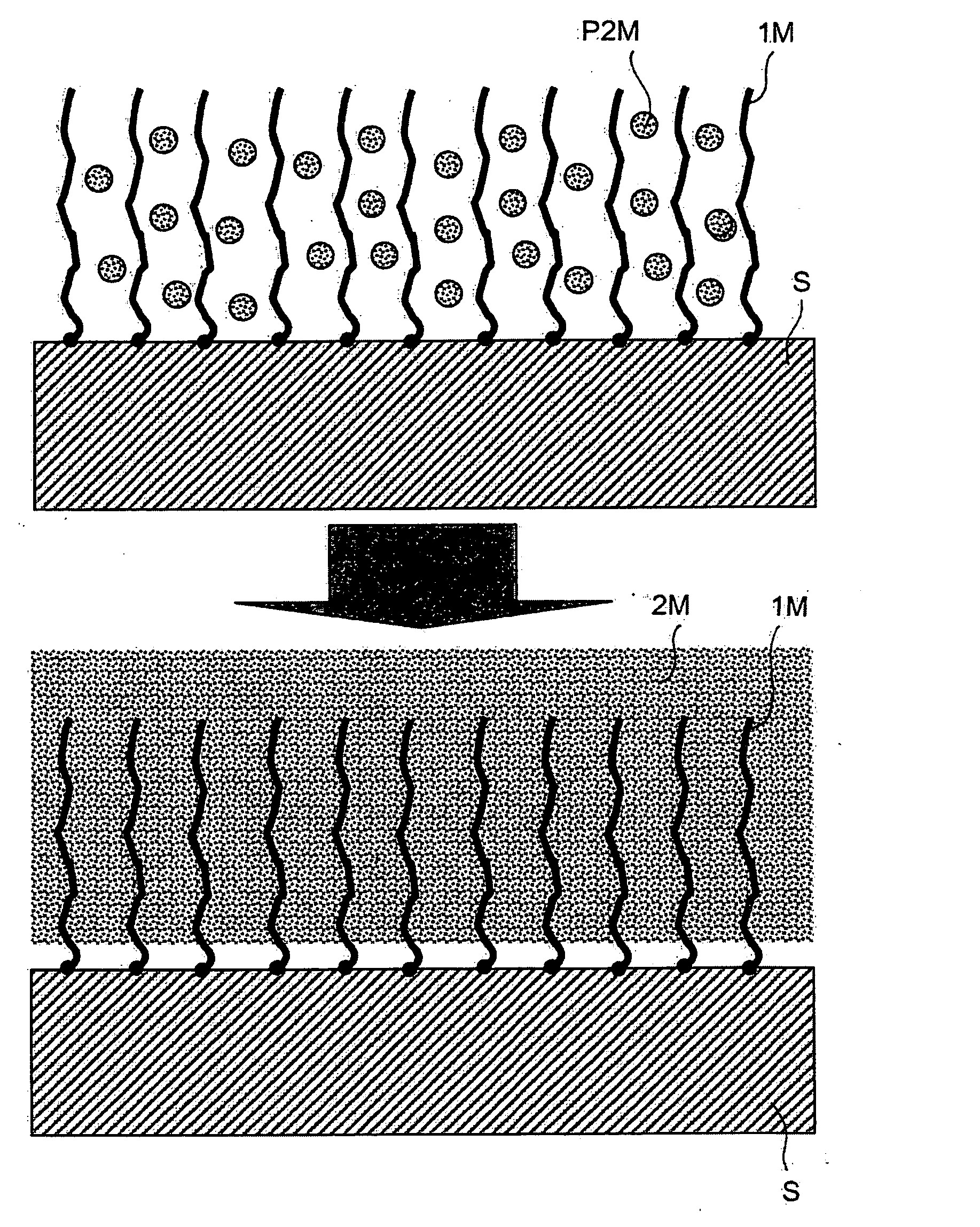
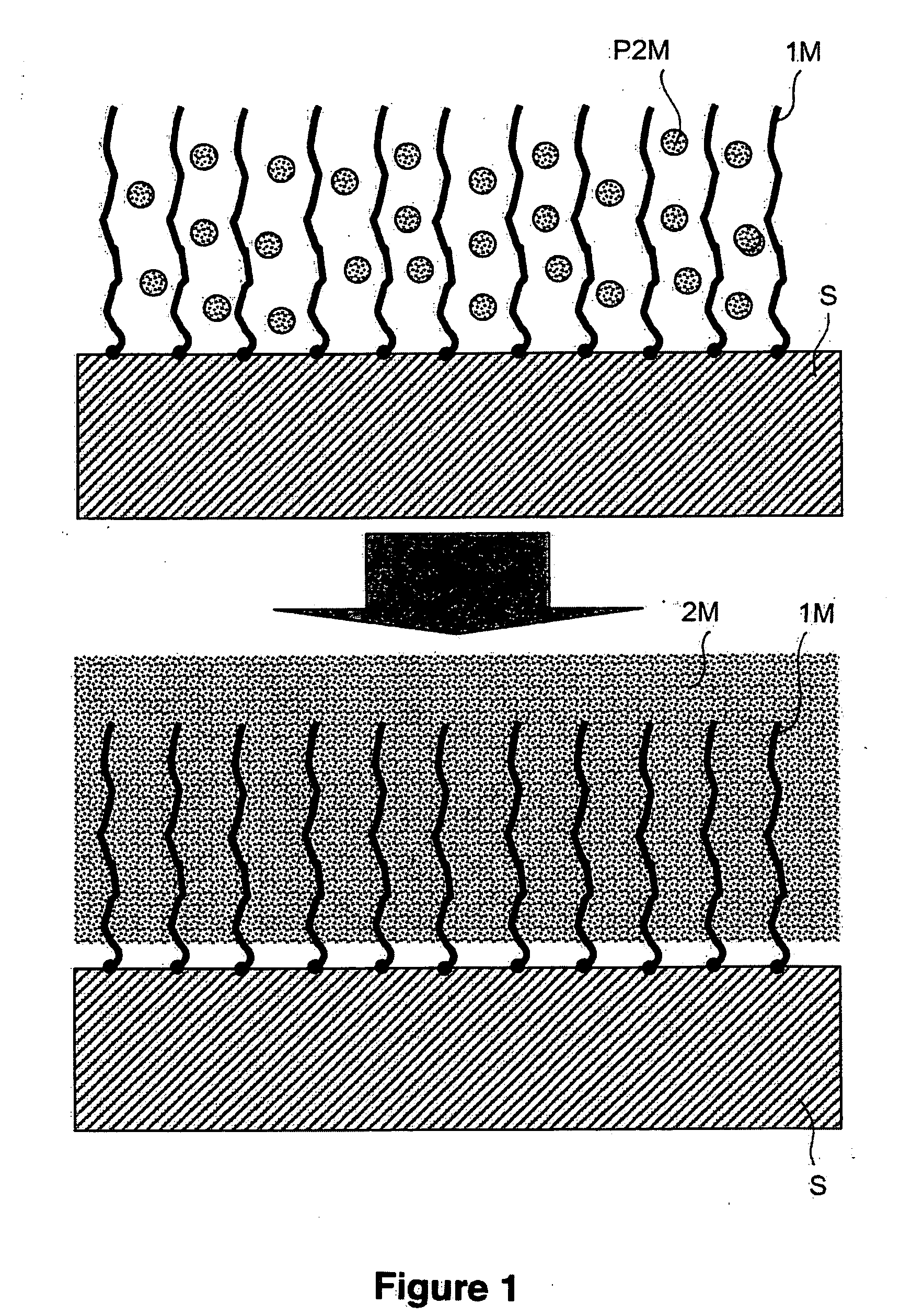
[0227] This example illustrates the very adhesive attachment of copper to a gold surface, using armouring consisting of an electrografted poly(4-vinylpyridine) (P4VP) film. FIG. 1 is a schematic representation of this example in accordance with the present invention.

[0228] An electrografted P4VP film 30 nm thick is first prepared on a 316L stainless-steel leaf subjecting the surface, dipped into a solution containing 40% by volume of 4-vinylpyridine in DMF, in the presence of 5×10⁻² mol / l of TEAP, to 50 voltammetric sweeps from −0.7 to −2.9 V / (Ag+ / Ag) at 200 mV / s.

[0229] The leaf thus treated is rinsed with DMF, dried under a stream of argon and then dipped for 25 minutes in a solution of 10 g of copper sulphate [CuSO4.5H2O] in 200 ml of deionized water. The leaf is then rapidly rinsed with a few jets of deionized water, and then dipped into DMF. It is then subjected to cathodic polarization at a ...

example 2

Attachment of Copper to a Gold Surface by Armouring Using an Electrografted P4VP Film (II)

[0235] The experiment of Example 1 is repeated, but using a different electrodeposition solution, which is conventional in spent-bath electroplating and also in barrel electroplating, providing a glossy deposit of copper of better quality. This example illustrates the compatibility of the armouring with electroplating processes, and thus makes it possible to benefit from reinforcement of the copper / gold interface while at the same time satisfactorily depositing the material of interest, consisting of the copper, according to the same process as usual.

[0236] To do this, the gold leaf covered with an electrografted P4VP film is dipped into an aqueous solution containing 50 ml of distilled water, 11 g of CuSO4.5H2O, 3 g of H2SO4 (d=1.83) and 6 mg of NaCl, for 30 minutes, and then electrolyzed in the solution for 15 seconds at the equilibrium potential, and then for 3 minutes at −0.5 V / (Ag+ / Ag) (...

example 3

Attachment of Nickel to a Gold Surface by Armouring by Means of an Electrografted P4VP Film

[0238] The same experiment as in Example 2 is performed, but using a reinforcing solution of nickel(II) ions, precursors of a deposit of metallic nickel, containing 50 ml of deionized water, 12.5 g of nickel sulphate, 3.25 g of nickel chloride and 2 g of boric acid.

[0239] A gold leaf covered with an electrografted P4VP film 30 nm thick is dipped into the solution thus prepared for 30 minutes, and then electrolyzed in the above solution for 15 seconds at the equilibrium potential, and then for 3 minutes at a cathode current density of between 2 and 4 A / dm2, with magnetic stirring.

[0240] A nickel deposit that shows good adhesion to the surface is obtained, since it withstands rinsing by ultrasound in DMF for 2 minutes, whereas the same deposit is impaired under the same rinsing conditions without prior armouring.


PUM

PropertyMeasurementUnit
Timeaaaaaaaaaa
Electrical conductoraaaaaaaaaa
Semiconductor propertiesaaaaaaaaaa

Abstract

The invention relates to the deposition or attachment of materials to surfaces. It relates to a process for coating a surface with a first material and a second material, comprising the following steps: placing the first material on the said surface, inserting into the first material placed on the said surface precursor molecules of the second material, converting the said precursor molecules of the second material inserted into the first material into the said second material such that this second material becomes formed on the said surface to be coated and within the said first material placed on the said surface. The object of the process of the invention is to allow the deposition of materials of any type onto surfaces of any type.

Description

TECHNICAL FIELD [0001] The invention relates to the deposition or attachment of materials onto surfaces. [0002] The invention relates in particular to a process for coating a surface, especially to a process for very adhesively depositing a material onto a surface. [0003] The process of the invention has the objective of producing an adhesive deposit of materials of any type onto surfaces of any type. PRIOR ART [0004] Numerous techniques have been described to date regarding the coating of surfaces in general, and in particular regarding the attachment of materials onto electrically conductive or semiconductive surfaces. The adhesive deposition of polymers onto electrically conductive or semiconductive surfaces, the adhesive deposition of metals onto electrically conductive or semiconductive surfaces, and the adhesive deposition of ionic insulators onto electrically conductive or semiconductive surfaces will be considered hereinbelow, in this order, in order to demonstrate the numer...

Claims


Application Information

Patent Timeline
IPC IPC(8): B05D5/00C09D5/44C23C26/00C25D3/38C25D5/34C25D5/54C25D15/00
CPCC09D5/4407C23C26/00C25D3/38Y10T428/12493C25D5/54C25D15/00C25D5/34C25D5/56C23C14/02B05D7/00
Inventor VIEL, PASCALAMEUR, SAMIBUREAU, CHRISTOPHE
Owner COMMISSARIAT A LENERGIE ATOMIQUE ET AUX ENERGIES ALTERNATIVES
Learn More