Alkali etching liquid for silicon wafer and etching method using same
a technology of etching liquid and silicon wafer, which is applied in the direction of surface treatment composition, decorative arts, chemistry apparatus and processes, etc., can solve the problems of lowering the mechanical strength of the wafer, affecting the uniformity of etching of the wafer surface, so as to suppress the diffusion of ions into the wafer interior, and reduce the level of ni contamination
Active Publication Date: 2006-06-15
SUMCO CORP
View PDF10 Cites 8 Cited by
- Summary
- Abstract
- Description
- Claims
- Application Information
AI Technical Summary
Benefits of technology
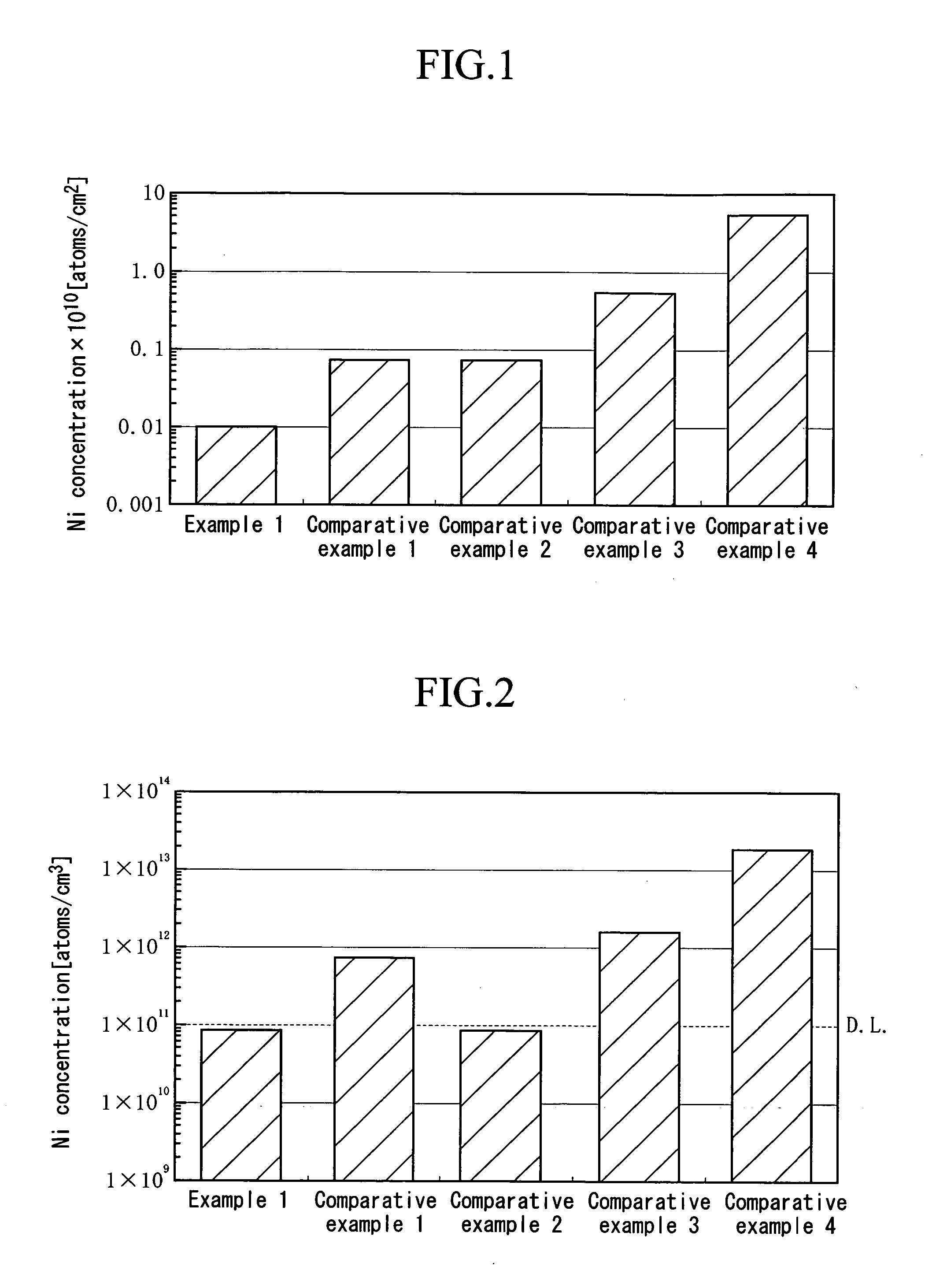
[0017] In this first aspect of the present invention, an aqueous solution of KOH is used as the primary component, and DTPA is then added to this KOH aqueous solution in a quantity within the range described above to form the alkali etching liquid. This alkali etching liquid contains between several dozen ppb and several hundred ppb of Ni, which is incorporated as an unavoidable impurity within the electronic industrial grade KOH aqueous solution used for etching semiconductor wafers, but this Ni can be adsorbed to the DTPA by bonding to the hydroxyl groups and amino groups of the DTPA. As a result, when the alkali etching liquid of the first aspect of the present invention is used for etching a silicon wafer or the like, the Ni ions within the KOH aqueous solution don't remain at the wafer surface without diffusing into the interior of the wafer, enabling a significant reduction in the Ni contamination of the silicon wafer caused by the alkali etching treatment.
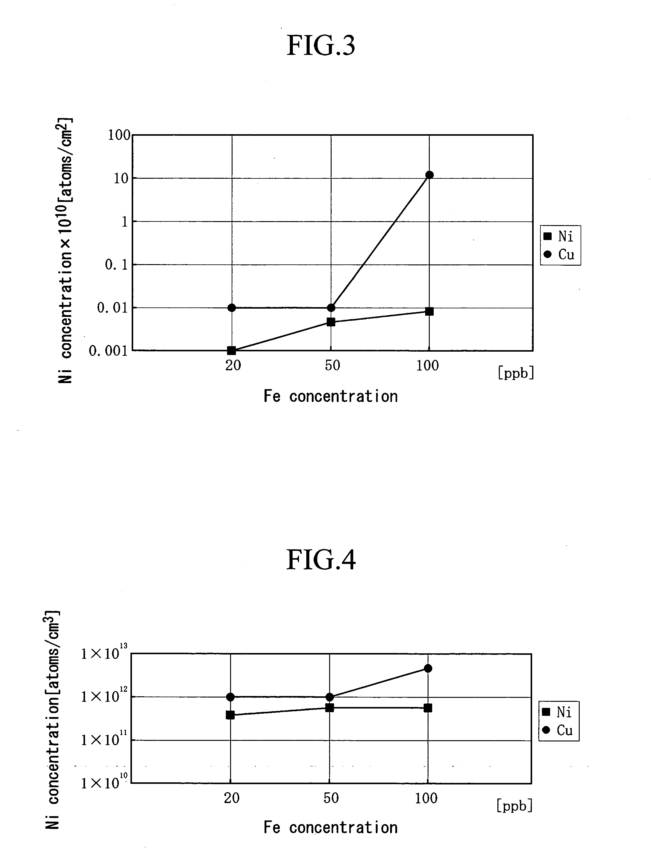
[0019] In this second aspect of the present invention, by conducting etching of a silicon wafer or the like using an etching liquid in which the Fe concentration within the KOH aqueous solution has been reduced to a level within the above range, Cu contamination of the silicon wafer can be prevented, and a further reduction in the level of Ni contamination can also be achieved.
[0023] In this fifth aspect of the present invention, even in the case of a silicon wafer with a resistivity of 1Ω·cm, which is particularly prone to the diffusion of Ni into the wafer interior, by using an alkali etching liquid according to any one of the first through fourth aspects, the Ni ions and Cu ions within the KOH aqueous solution don't remain at the wafer surface, meaning diffusion of these ions into the wafer interior can be suppressed dramatically, and enabling a reduction in the Ni contamination of the silicon wafer, and prevention of the Cu contamination caused by the alkali etching.
[0025] An alkali etching liquid for silicon wafers according to the present invention uses a KOH aqueous solution as the primary component, and includes a predetermined quantity of DTPA added to this KOH aqueous solution. The electronic industrial grade KOH aqueous solution used for etching semiconductor wafers contains between several dozen ppb and several hundred ppb of Ni as an unavoidable impurity, but this Ni is adsorbed to the DTPA, meaning when the alkali etching liquid of the present invention is used for etching a silicon wafer or the like, the Ni ions within the KOH aqueous solution don't remain at the wafer surface, meaning diffusion of these ions into the wafer interior can be suppressed dramatically, and enabling a reduction in the Ni contamination of the silicon wafer caused by the alkali etching treatment. Furthermore, by conducting etching of a silicon wafer or the like using an alkali etching liquid in which the Fe concentration within the KOH aqueous solution has been reduced to a level within the range described above, Cu contamination of the silicon wafer can be prevented, and a further reduction in the level of Ni contamination can also be achieved. Moreover, according to an etching method of the present invention, even in the case of a silicon wafer with a resistivity of 1Ω·cm, which is particularly prone to the diffusion of Ni into the wafer interior, by using an alkali etching liquid according to the present invention, the Ni ions and Cu ions within the KOH aqueous solution don't remain at the wafer surface, meaning diffusion of these ions into the wafer interior can be suppressed dramatically, and enabling a reduction in the Ni contamination of the silicon wafer, and prevention of the Cu contamination caused by the alkali etching.
Problems solved by technology
This affected layer can cause a variety of problems, including inducing crystal defects such as slip dislocation in subsequent device production processes, lowering the mechanical strength of the wafer, and causing undesirable effects on the electrical properties of the wafer, and must consequently be completely removed.
Acid etching has a faster etching rate, meaning uniform etching of the wafer surface is more difficult, and as a result, it tends to be prone to a deterioration in the degree of smoothness of the lapped wafer.
However, the electronic industrial grade alkali solutions used in this type of alkali etching contains between several dozen ppb and several ppm of metal impurities.
If an alkali solution containing these types of metal impurities is used, as is, as the alkali treatment liquid within a wafer etching step, then during etching, metal ions from the metal impurities may adhere to the wafer surface or diffuse into the wafer interior, causing a deterioration in the wafer quality, which can cause a marked deterioration in the properties of the semiconductor device formed using the wafer.
However, commercially available high purity alkali solutions are limited to the extremely expensive analytical grade alkali solutions, and the use of such solutions for industrial purposes is completely impractical from a cost perspective.
However, even using the etching methods and etching liquids disclosed in the above patent references 1 to 3, the reduction in the quantity of metal contaminants that diffuse into the interior of the wafer during etching is still not entirely satisfactory, and further improvements are desirable.
Method used
View moreImage
Smart ImageViewing Examples

Examples
example 1
[0036] A 40% by weight aqueous solution of KOH was prepared. This KOH aqueous solution contained 10 ppb of Ni. DTPA was added to, and mixed into this KOH aqueous solution in a quantity equivalent to 0.1 g / L, thereby forming an alkali etching liquid.
Login to View More PUM
| Property | Measurement | Unit |
|---|---|---|
| resistivity | aaaaa | aaaaa |
| resistivity | aaaaa | aaaaa |
| resistivity | aaaaa | aaaaa |
Abstract
An alkali etching liquid for a silicon wafer that includes an aqueous solution of potassium hydroxide, and from 0.1 g / L to 0.5 g / L of diethylene triamine pentaacetic acid. Furthermore, the Fe concentration of the aqueous solution of potassium hydroxide is no more than 50 ppb. An etching method that including a step of etching a silicon wafer with a resistivity of no more than 1Ω·cm using the etching liquid.
Description
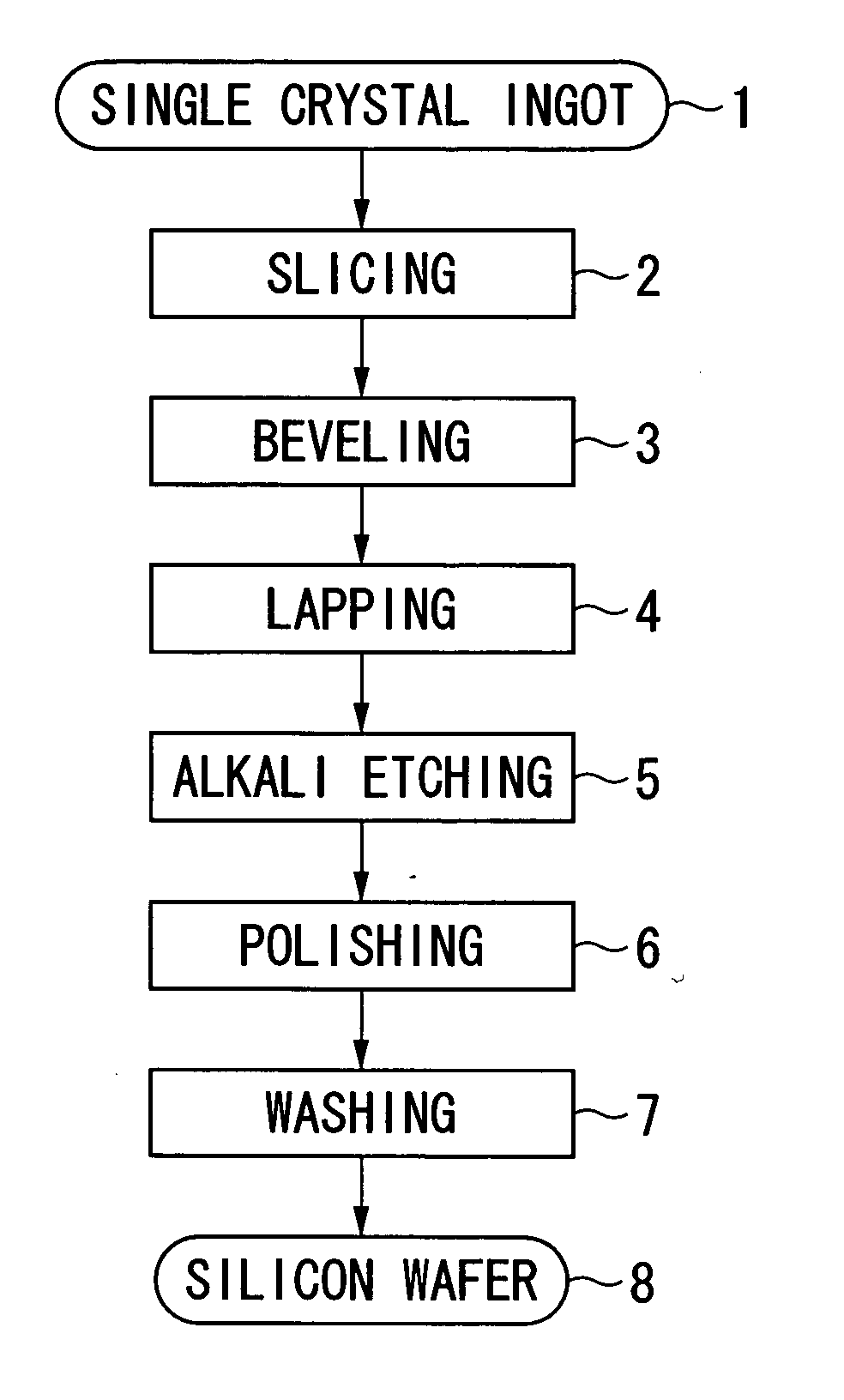
BACKGROUND OF THE INVENTION [0001] 1. Field of the Invention [0002] The present invention relates to an alkali etching liquid which exhibits a Ni contamination reduction effect and a Cu contamination prevention effect even during the alkali etching of silicon wafers of low resistivity, and also relates to an etching method using such an etching liquid. [0003] Priority is claimed on Japanese Patent Application No. 2004-357521, filed Dec. 10, 2004, the content of which is incorporated herein by reference. [0004] 2. Description of Related Art [0005] In a typical silicon wafer production, as shown in FIG. 5, a silicon single crystal ingot 1 that has been drawn using an apparatus for pulling single crystal is cut into blocks of a specified size, further grinding of the outer diameter is performed, and the resulting ingot block is then subjected to a wafer cutting (slicing) step 2, thereby forming thin, disc-like wafers. An internal diameter saw, band saw, or wire saw or the like is used ...
Claims
Login to View More Application Information
Patent Timeline
 Patent Type & Authority Applications(United States)
IPC IPC(8): C09K13/00C03C15/00B44C1/22C25F3/00
CPCC09K13/02H01L21/02019H01L21/30608
Inventor NAKASHIMA, TAKAHISATAKEMURA, MAKOTOHASHIMOTO, YASUYUKI
Owner SUMCO CORP
Features
- R&D
- Intellectual Property
- Life Sciences
- Materials
- Tech Scout
- Unparalleled Data Quality
- Higher Quality Content
- 60% Fewer Hallucinations
Learn More Browse by: Latest US Patents, China's latest patents, Technical Efficacy Thesaurus, Application Domain, Technology Topic, Popular Technical Reports.
© 2025 PatSnap. All rights reserved.Legal|Privacy policy|Modern Slavery Act Transparency Statement|Sitemap|About US| Contact US: help@patsnap.com