


Quick Research
Generate reliable direction feasibility study reports for your R&D in just a few steps.

Technical Q&A
Discover and master advanced knowledge NOW. Basics, ideas, possibilities, all at once.

Find Solutions
As an expert in R&D theories, this can generate solutions to your technical problems instantly.

Evaluate Feasibility
Analyze your overall solution with one click, know your potential R&D risks in advance.

Monitor Landscape
Get weekly tech updates, stay abreast of the latest tech innovations and key insights.
Flexible multilayer wiring board and manufacture method thereof
a multi-layer wiring and flexible technology, applied in the direction of printed element electric connection formation, semiconductor/solid-state device details, conductive pattern formation, etc., can solve the problems of difficult to ensure the mounting accuracy of semiconductor packages, difficult to produce high-density wiring with a line/space width of 25 m/25 m or less, and difficulty in ensuring the flatness of external terminals. , to achieve the effect of reducing size and weight, reducing thickness and reducing thickness
- Summary
- Abstract
- Description
- Claims
- Application Information
AI Technical Summary
Benefits of technology
Problems solved by technology
Method used
Image

Examples
example 1
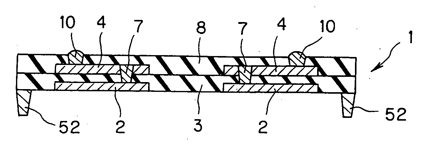
[0055] A copper substrate having a thickness of 0.125 mm (EFTEC64T produced by Furukawa Electric Co., Ltd.) was prepared as a conductive substrate and a resist (HTB-120N produced by JSR Corporation) was applied onto the copper substrate, then a predetermined resist pattern was formed. Subsequently, using the copper substrate as a power feeding layer and the resist pattern as a mask, a nickel plating layer (thickness: 2 μm), a gold plating layer (thickness: 1 μm), a nickel plating layer (thickness: 2 μm) and a copper plating layer (thickness: 5 μm) were stacked by electrolytic plating in the order named, thereby to form the first layer circuit wiring of a four-layer structure. Thereafter, the resist pattern was removed. This first-layer circuit wiring had a line / space width of 10 μl / 10 μm. (hereinabove, First Process)
[0056] Then, an insulating sheet (thickness: 35 μm; Bonding Sheet produced by Nippon Steel Chemical Co., Ltd.) and copper foil (thickness: 3 μm; produced by Mitsui Mini...
example 2
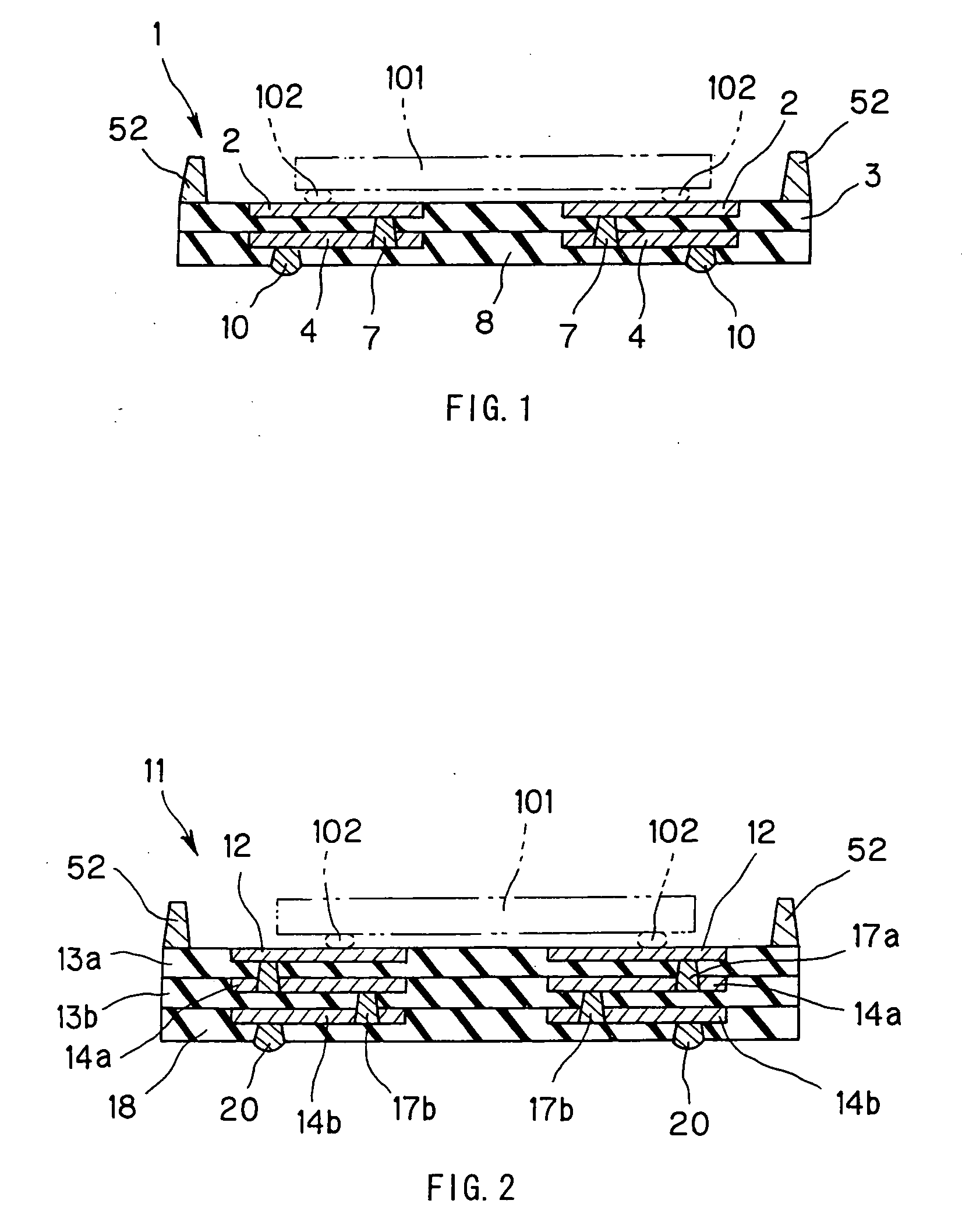
[0064] Through the first process like in Example 1, the first layer circuit wiring having a line / space width of 10 μm / 10 μm was formed on a copper substrate.
[0065] Then, by repeating twice the second to fourth processes of Example 1, the second layer circuit wiring and the third layer circuit wiring were formed and interlayer connection between the layers was carried out. Each of the second layer circuit wiring and the third layer circuit wiring thus formed had a line / space width of 15 μm / 15 μm.
[0066] Thereafter, like in the fifth process of Example 1, an insulating layer and external connection terminals were formed on the third layer circuit wiring. Then, like in the sixth process of Example 1, the copper substrate was etched to form an outer frame.
[0067] Through the foregoing processes, there was obtained the flexible multilayer wiring board having the three-layer structure as shown in FIG. 2 and having the line / space widths falling within the range of 5 μm / 5 μm to 25 μm / 25 μm...
PUM
| Property | Measurement | Unit |
|---|---|---|
| thickness | aaaaa | aaaaa |
| thickness | aaaaa | aaaaa |
| thickness | aaaaa | aaaaa |
Abstract
Description
Claims
Application Information
 - R&D Engineer
- R&D Manager
- IP Professional
- Industry Leading Data Capabilities
- Powerful AI technology
- Patent DNA Extraction
Browse by: Latest US Patents, China's latest patents, Technical Efficacy Thesaurus, Application Domain, Technology Topic, Popular Technical Reports.
© 2024 PatSnap. All rights reserved.Legal|Privacy policy|Modern Slavery Act Transparency Statement|Sitemap|About US| Contact US: help@patsnap.com