
High frequency switching circuit device

a high-frequency switching and circuit device technology, applied in the field of high-frequency switching circuit devices, can solve the problems of difficult to provide both low insertion loss and high isolation, and the phone is not suitable for portable devices, and achieves the effects of reducing the number of package pins and the package size, enhancing operability, and miniaturizing cellular phones

Inactive Publication Date: 2006-01-05
COLLABO INNOVATIONS INC
View PDF4 Cites 31 Cited by
  • Summary
  • Abstract
  • Description
  • Claims
  • Application Information

AI Technical Summary

Benefits of technology

[0031] An object of the present invention is to solve the above described problems and provide a high frequency switching circuit device where a switch element can be controlled with precision without an increase in the chip size, deterioration of frequency characteristics of the insertion loss of an ON path, or an increase in the number of control signals that are to be inputted through external pins.
[0032] Another object of the present invention is to provide a high frequency switching circuit device for implementing a compact and lightweight antenna switch for use in a compact and lightweight cellular phone, even when the number of bands is further increased in the development of cellular phones.
[0033] Still another object of the present invention is to provide a high frequency switching circuit device having high performance by securing high isolation, which is difficult to achieve in the case of multiple bands.
[0049] As described above, a high frequency switching circuit device according to the present invention uses diodes made of Schottky junctions that can be fabricated at the same time in an FET fabricating process, in such a manner that a diode logic circuit for logical synthesis of voltages from a number of control voltage input terminals, for example, for selecting and outputting the highest voltage from among, for example, a number of control voltage input terminals is integrally formed on a compound semiconductor substrate. As a result, a shunt switching element for securing isolation can be controlled by the voltage at the control voltage input terminal of the series switching element, and the control system and the like can be miniaturized, in comparison with the prior art. Therefore, the number of package pins and the package size are reduced, and operability is enhanced when the number of bands of cellular phones is increased, and the invention can contribute to the miniaturization of cellular phones.
[0050] In addition, this diode logic circuit is connected to a source or a drain of the FET's that form the switching element, that is to say, to the middle connection point of the series circuit of the number of FET's, and thereby, the potential can be fixed without adding a power supply terminal. As a result of this, a high frequency switching circuit device having excellent properties, such as low insertion loss, high isolation and low distortion, can be implemented.
[0051] In addition, in the case where the power that is handled differs depending on the path that is switched as a result of transmission / reception switching, some field effect transistor stages on the reception side handling low power are shared, and furthermore, these shared field effect transistor stages are controlled by a diode logic circuit, and thereby, the chip size can be reduced without increasing the number of control systems, and the invention can further contribute to the miniaturization of cellular phones.

Problems solved by technology

However, the volume and the weight increase in proportion to the number of systems with which the phone can be used.
Such a phone is not suitable as a portable device.
On the other hand, in the case where such GaAs FET's are used for a switching element, a problem rises where it is difficult to provide both low insertion loss and high isolation.
In the case where the width of the gate voltage terminal is reduced, however, a problem arises where ON resistance increases, and therefore, insertion loss increases.
Accordingly, it is difficult to provide both low insertion loss and high isolation.
Though as described above, it is difficult to provide low insertion loss and high isolation in a single FET, this problem has been solved by combining FET's.
As a result, a problem arises where the number of pins for the package of the high frequency switching circuit device increases and the size of the package increases, and thus, the configuration is unsuitable for a portable terminal where miniaturization of the device is required.
According to the above described methods, however, the following problems arise.
Therefore, frequency properties of the insertion loss of the ON path deteriorate.
In addition, according to the second method, it is extremely difficult to fabricate a differential amplifier circuit and an inverter circuit within a GaAs chip.

Method used


Image

  • High frequency switching circuit device
  • High frequency switching circuit device
  • High frequency switching circuit device

Examples


embodiment 1

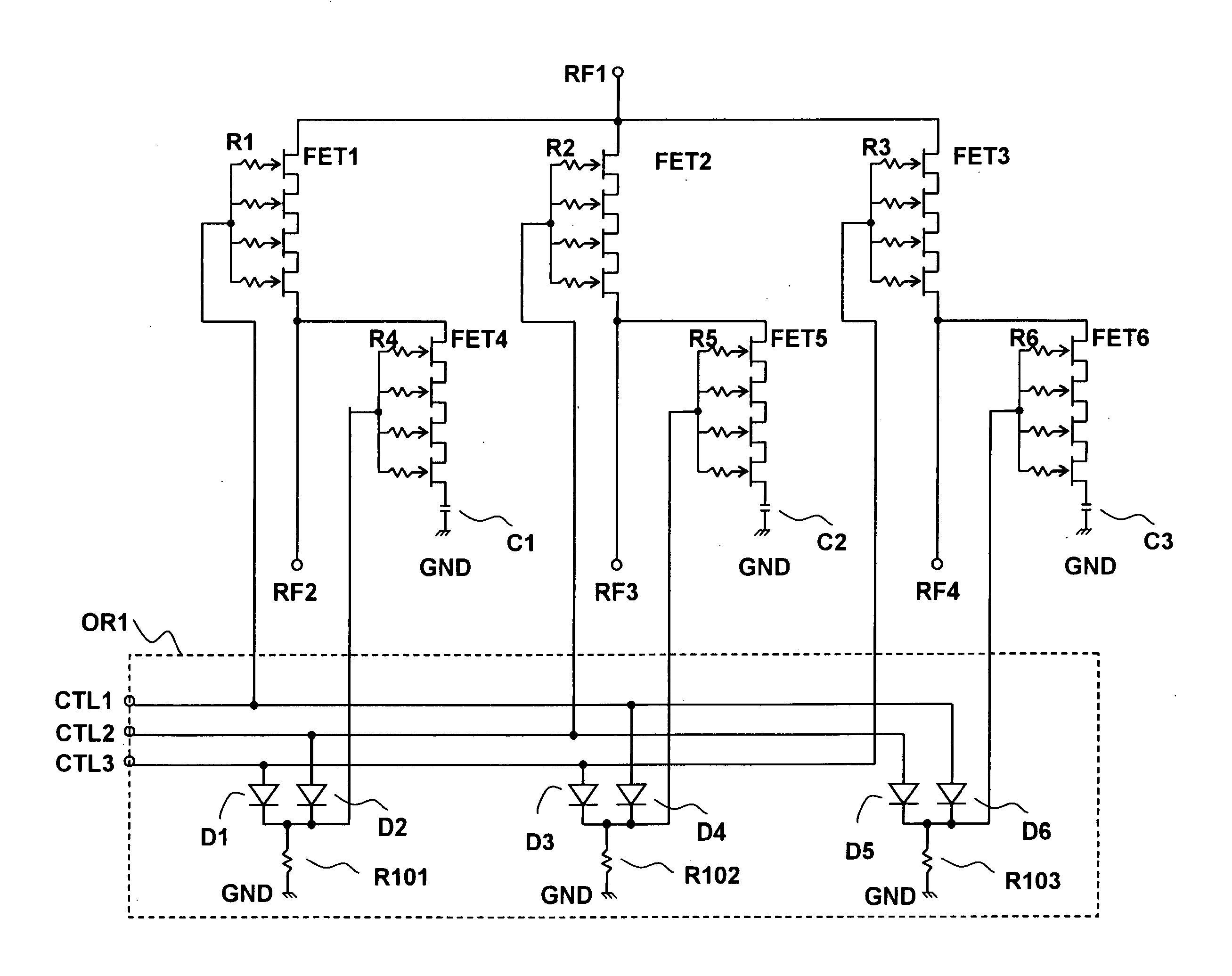
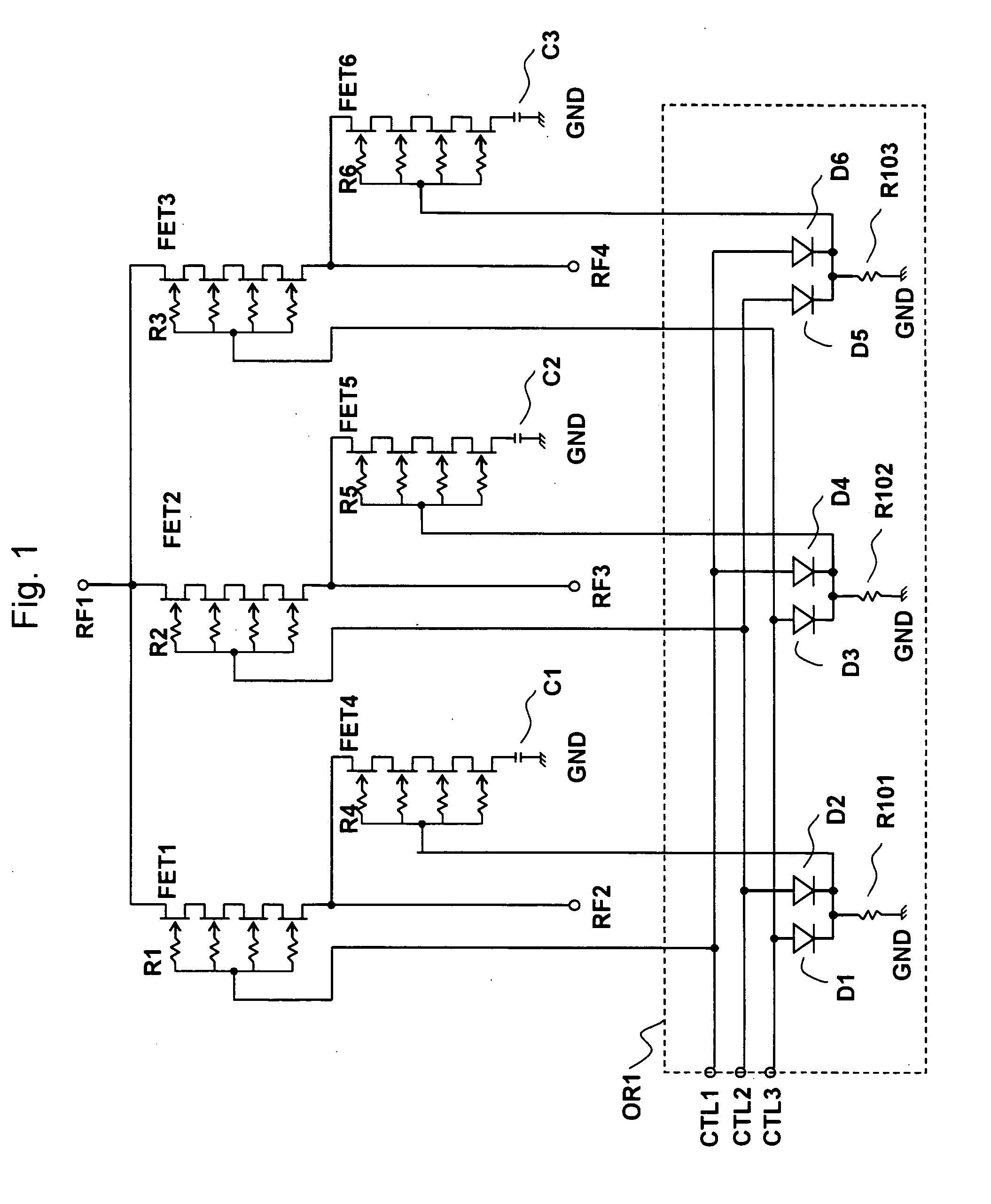
[0070]FIG. 1 is a circuit diagram showing an example of a high frequency switching circuit device according to Embodiment 1 of the present invention, and concretely shows a circuit configuration of an SP3T switch for high frequency.

[0071] In FIG. 1, first high frequency signal terminal RF1 to fourth high frequency signal terminal RF4, first field effect transistor stage FET1 to sixth field effect transistor stage FET6, as well as control voltage input terminals CTL1 to CTL3, are the same as those according to the prior art. First diode D1 to sixth diode D6 are diodes that form a diode logic circuit OR1, and have been prepared as metal-semiconductor Schottky junctions, of the same material as the gate electrodes of metal-semiconductor FET's. These diodes can be fabricated at the same time in an FET fabricating process.

[0072] The anode of first diode D1 is connected to third control voltage input terminal CTL3, and the cathode is connected to the gate voltage terminal of fourth fiel...

embodiment 2

[0085]FIG. 4 is a diagram showing an example of a high frequency switching circuit device according to Embodiment 2 of the present invention. FIG. 4 concretely shows the circuit configuration of an SP3T switch for high frequency.

[0086] In FIG. 4, first high frequency signal terminal RF1 to fourth high frequency signal terminal RF4, first field effect transistor stage FET1 to sixth field effect transistor stage FET6, and control voltage input terminals CTL1 to CTL3 are the same as those according to the prior art. First diode D1 to sixth diode D6 are the same as those in Embodiment 1. First diode D1 to ninth diode D9 are diodes that form a diode logic circuit OR2, and are made of Schottky junctions that can be fabricated of the same material and at the same time as the gate electrode of a metal-semiconductor FET in an FET fabricating process.

[0087] The anodes of seventh diode D7, eighth diode D8 and ninth diode D9 are connected to first control voltage input terminal CTL1, second c...

embodiment 3

[0093]FIG. 6 is a diagram showing an example of a high frequency switching circuit device according to Embodiment 3 of the present invention. Concretely speaking, FIG. 6 shows the circuit configuration of an SP3T switch for high frequency.

[0094] In FIG. 6, first high frequency signal terminal RF1 to fourth high frequency signal terminal RF4, first field effect transistor stage FET1 to sixth field effect transistor stage FET6, and control voltage input terminals CTL1 to CTL3 are the same as those according to the prior art. First diode D1 to sixth diode D6 are diodes that form diode logic circuit OR1, which is the same as that of Embodiment 1.

[0095] In the circuit configuration of the SP3T switch for high frequency according to the present Embodiment 3, the gate voltage terminal of first field effect transistor stage FET1 is connected to the middle connection point of a number of field effect transistors that form fourth field effect transistor stage FET4, via resistor R204. In the...


PUM


Abstract

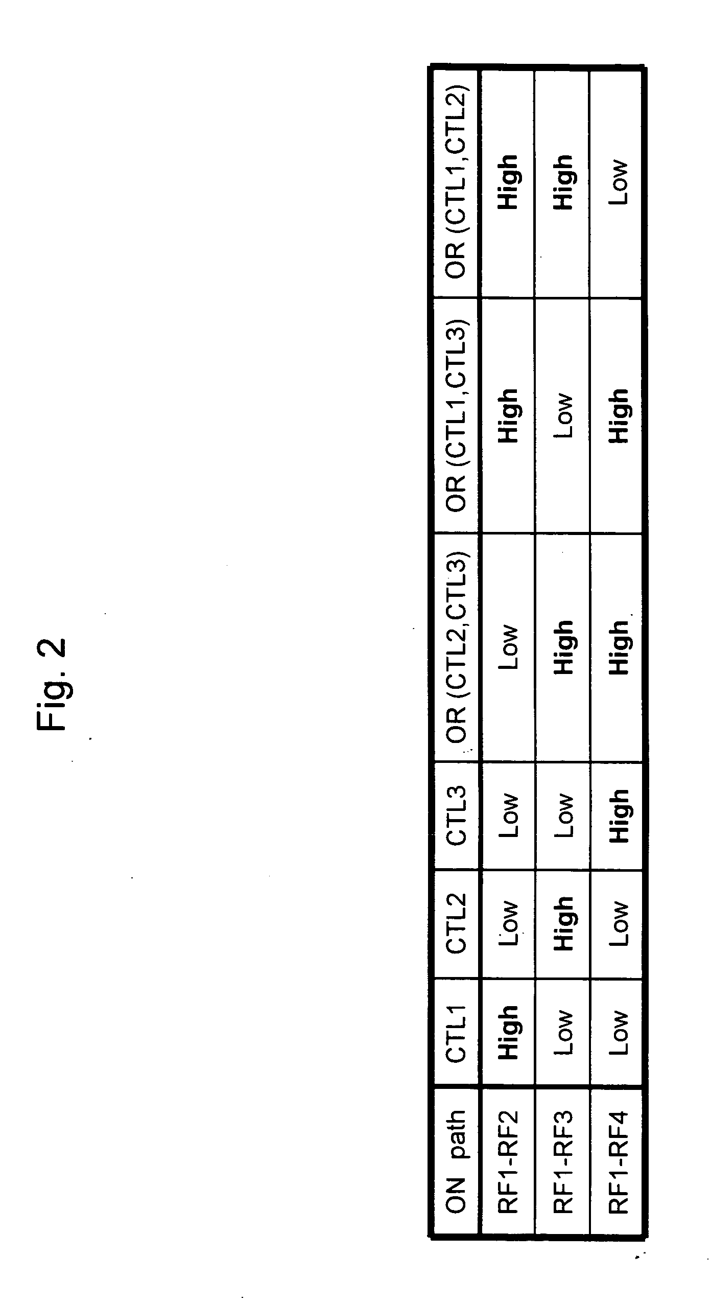
A diode logic circuit which can select a high voltage from among the voltages of a number of control voltage input terminals using a number of diodes made of Schottky junctions is integrally formed on a compound semiconductor substrate on which MESFET stages for switching and for securing isolations have been formed. In addition, the MESFET stages for switching are controlled by the voltages of the number of control voltage input terminals and the MESFET stages for securing isolations are controlled by the OR voltage that is outputted from the diode logic circuit.

Description

BACKGROUND OF THE INVENTION [0001] 1. Field of the Invention [0002] The present invention relates to a high frequency switching circuit device which is made of metal-semiconductor field effect transistor stages formed on a compound semiconductor substrate, and which is appropriate for use in a communication terminal device, such as a cellular phone. [0003] 2. Prior Art [0004] Accessing styles and radio transmission frequencies differ, depending on the standard in communication systems for cellular phones. Therefore, it is necessary to carry around cellular phones that conform to the respective standards of the country or region where the service is utilized, or to carry around one multi-band cellular phone which can be used with a number of communication systems, in order to be able to utilize a cellular phone in a number of regions in the world. [0005] In the latter case, a cellular phone may be formed of parts that have been manufactured for the respective communication systems, s...

Claims


Application Information

Patent Timeline
Patent Type & Authority Applications(United States)
IPC IPC(8): H03K17/62
CPCH03K17/693H03K17/00
Inventor YASUDA, EIJIHIDAKA, KENICHIMASUMOTO, YASUYUKINAKATSUKA, TADAYOSHIWATANABE, ATSUSHITARA, KATSUSHI
Owner COLLABO INNOVATIONS INC
Learn More