
Clock synchroniser and clock and data recovery apparatus and method

a clock synchroniser and data recovery technology, applied in multiplex communication, baseband system details, instruments, etc., can solve the problems of inability to recover small amounts of jitter, inability to accept data error rates in received data, and inability to add additional jitter in the data stream, so as to avoid data loss, reduce jitter, and reduce jitter

Inactive Publication Date: 2005-10-06
WOLFSON MICROELECTRONICS LTD
View PDF16 Cites 74 Cited by
  • Summary
  • Abstract
  • Description
  • Claims
  • Application Information

AI Technical Summary

Benefits of technology

[0032] It should be noted that there is a subtle distinction between the remote clock, i.e. the clock as observable at the transmitter, and the received clock, i.e. the clock observable at the receiver. The long-term average frequency of the two is equal, so if a local clock is synchronised to the received clock, it is also synchronised to the remote clock. However, it is the received clock, with additional short-term jitter as described above, which is actually used in any signal processing at the receiver, and the receiver embodying the present invention attenuates this undesirable jitter and provides a reduced-jitter local clock signal and retimed data output stream.
[0110] Embodiments of the invention may be used in data receiver circuits and provide the advantage that they generate a clean clock locally and retime the incoming data to this clock prior to a digital-to-analogue converter to avoid clock-jitter induced noise and distortion. The local clock and the incoming data clock are synchronised and data loss is avoided.

Problems solved by technology

Additional jitter in the data stream may be introduced by inter-symbol interference due to the finite bandwidth of the transmission channel or by crosstalk between adjacent cables.
For general data links, increasing amounts of jitter may only cause problems if they lead to unacceptable data error rates in the received data.
However for audio data links, even small amounts of jitter may be important, since the digital audio signal will eventually be reproduced as an analogue waveform by a digital-analogue converter (DAC).
For high quality reproduction of the digital audio a significant amount of jitter will impair the performance.
Long-term, both crystals will have a frequency error (possibly 500 ppm) and there may also be an error in the frequency generated by the PLL at either end.
If the transmitter clock is faster than the receiver clock, data will occasionally be lost: if the receiver clock is faster than the transmitter clock occasional bits will be sampled and clocked out twice.
Even a few ppm difference on a 12 MHz data stream could give missing bits several times a second, which would be completely unacceptable for both digital audio data or indeed more general data streams.
However, in this implementation the elastic buffer is used merely to absorb the short- and medium-term jitter and no effort is made to synchronise the local clock to the remote clock, i.e. no measures are taken to ensure the respective data rates are the same long term, to avoid loss of data.
However for systems with no IDLE data this system will results in corrupted and / or lost data.
Thus, the circuits disclosed in U.S. Pat. No. 6,594,329 may be used in asynchronous data systems, but cannot be used in synchronous systems, such as audio systems, where input and output sample rates do have to be equal long-term.
However, the consequent large steps in the VCO output frequency makes these types of circuits unsuitable for synchronous systems.
This increases the complexity and cost of the system, and there still remains the problem of jitter on the “local clock” generated by the VCO
However for a non-rational frequency difference the phase will be constantly adjusting to keep track and this will result in a jittery local clock.
No data loss will occur but the recovered clock will not be suitable for use with a DAC.
These off-chip components increase the cost and physical size of the design.
They can also degrade the performance unless great care is exercised.
Ground bounce’, or momentary differences between the ground off- and on-chip, is hard to reduce in a practical IC package design, and can possibly even introduce more jitter than the loop filter is attenuating from the remote clock.
Also if the bandwidth of the receiving PLL is too small, it may be unable to respond quickly enough to track large short-term jitter well enough to recover the data properly.
The low-bandwidth loop still receives a signal with a large amount of jitter from the high-bandwidth loop, so may occasionally lose lock unless design compromises are made with its performance.

Method used


Image

  • Clock synchroniser and clock and data recovery apparatus and method
  • Clock synchroniser and clock and data recovery apparatus and method
  • Clock synchroniser and clock and data recovery apparatus and method

Examples


Embodiment Construction

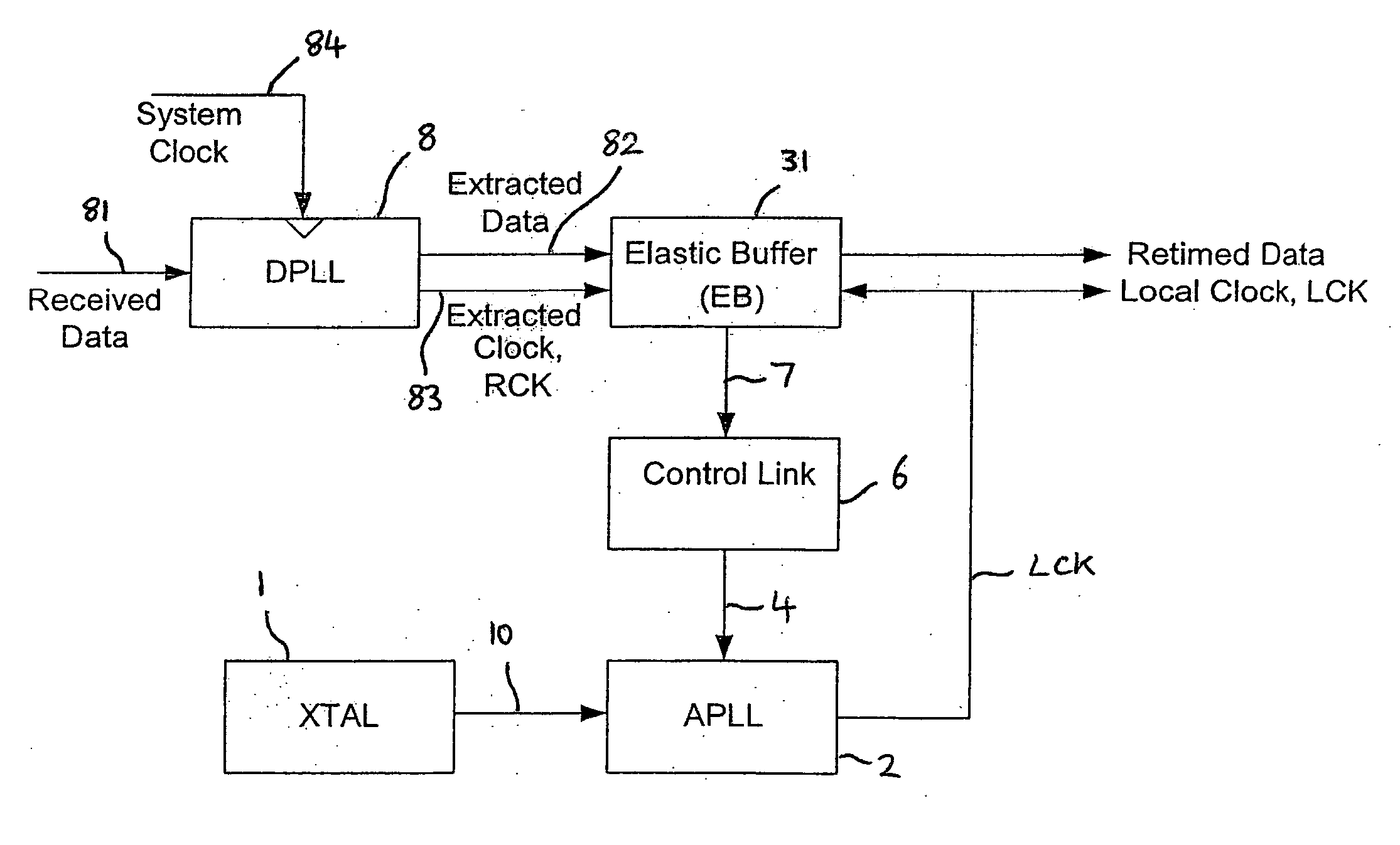
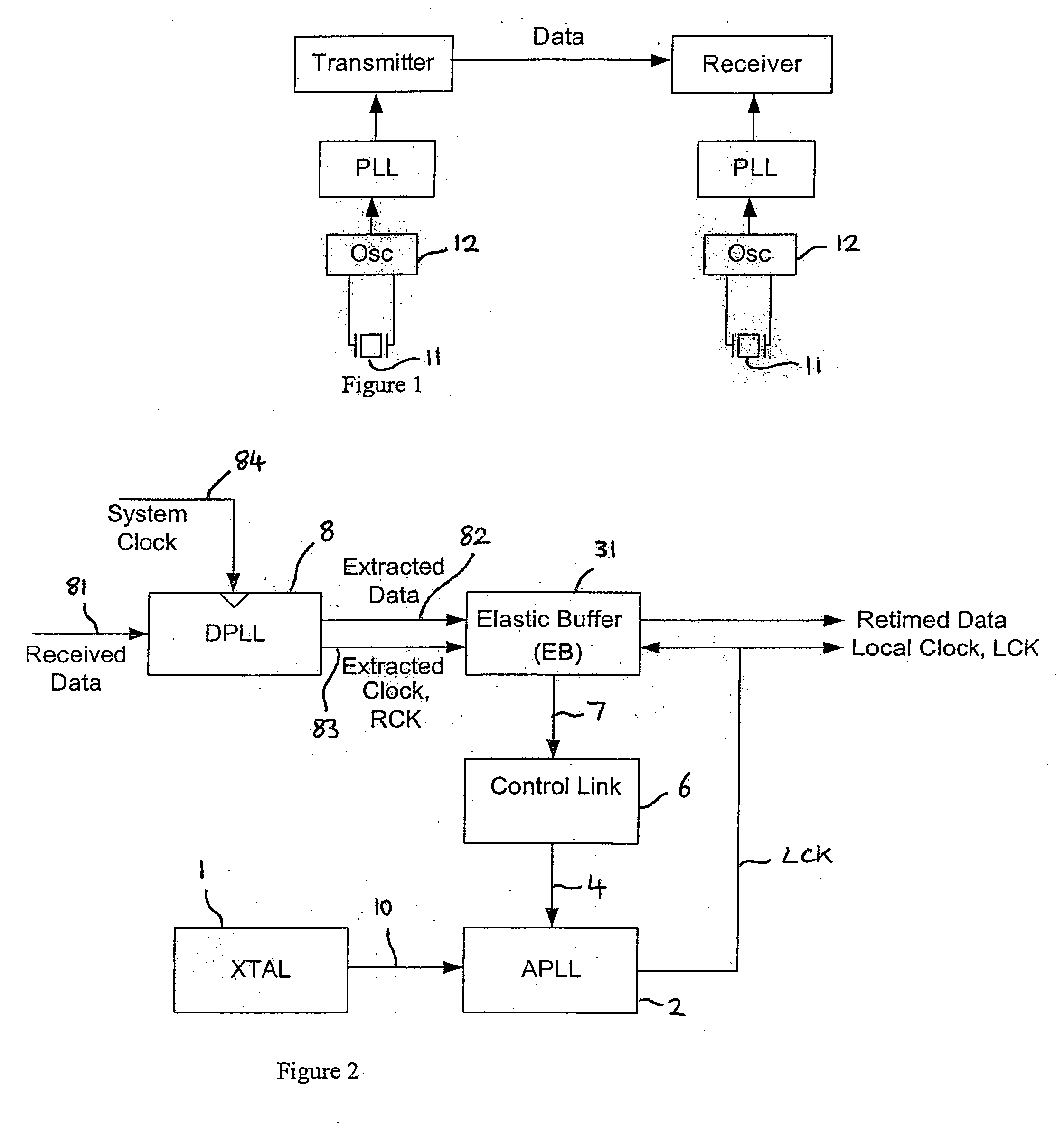
[0123] Referring now to FIG. 2, a clock and data recovery circuit (system) embodying the invention includes a clock and data extraction circuit 8 that comprises a digital phase locked loop (DPLL). A stream of received data 81 containing embedded clock information is supplied to the DPLL, which is used to lock onto the incoming data and generate an internal intermediate clock RCK 83 (which shall be referred to as the received clock) and a stream of retimed internal data 82 (i.e. extracted data). The generation of the internal intermediate clock may also be described as the extraction of a clock signal from the stream of received data, and hence the internal intermediate clock may also be referred to as an extracted clock.

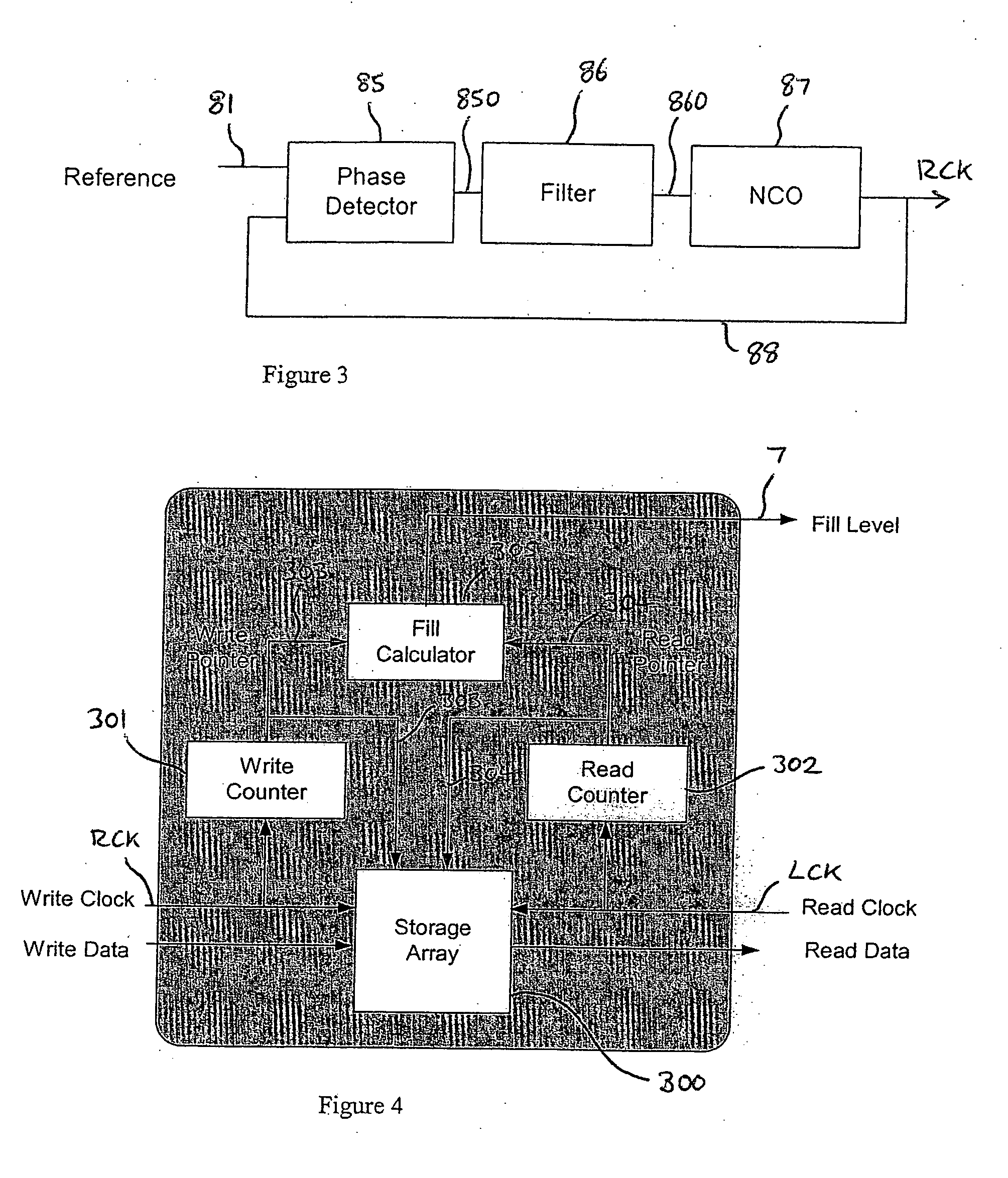
[0124] The extracted data 82 and the extracted clock 83 are provided to inputs of an elastic buffer (EB) 31. The EB is used to absorb any short or medium term timing variations between the local and remote clock domains. It also generates a pointer error signal (P) ...


PUM


Abstract

A clock synchroniser, and clock and data recovery apparatus incorporating the clock synchroniser, are described, together with corresponding clock synchronisation methods. The clock synchroniser incorporates an elastic buffer. A received clock signal is used to clock data into the buffer, and a locally generated clock is used to clock data out of the buffer. The local clock is synthesised using a PLL, and a fill-level signal from the elastic buffer is used to control to local clock frequency to maintain a desired average quantity of data in the buffer, thereby achieving synchronisation of the received and local clocks. In preferred embodiments the fill-level signal is used to control a variable divider in the feedback path of the PLL, which is supplied with a highly stable reference signal. A synchronised, and low-jitter local clock is thus produced. Preferably, the elastic buffer employs counters of relatively wide word width, and a storage array of much reduced depth, read and write pointers being provided by just a few of the least significant bits of the words.

Description

FIELD OF THE INVENTION [0001] The present invention relates to clock synchronisers and to clock and data recovery apparatus and methods. Particular embodiments are concerned with methods and circuits for recovering a low jitter clock and data from jittered data (e.g. a jittery data stream). BACKGROUND TO THE INVENTION [0002]FIG. 1 shows a data link comprising two systems each clocked by a respective PLL. The transmitter transmits data at a given rate and the receiver clocks the data in using its local clock. However the two clock frequencies may not be exactly the same, either short-term or long-term. [0003] Short-term variations in frequency will arise in each clock from thermal noise or external interference, and can be considered as jitter in the respective clocks. Additional jitter in the data stream may be introduced by inter-symbol interference due to the finite bandwidth of the transmission channel or by crosstalk between adjacent cables. [0004] For general data links, increa...

Claims


Application Information

Patent Timeline
IPC IPC(8): G06F5/06G06F5/12H03L7/10H03L7/197H04J3/06H04L7/00H04L7/033H04L25/05
CPCG06F5/06G06F5/12H04J3/0632H03L7/10H03L7/197G06F2205/061H03L7/1075H04L7/00
Inventor LESSO, PAUL
Owner WOLFSON MICROELECTRONICS LTD
Learn More