
Substrate

a technology of substrate and ceramic base, which is applied in the field of substrate, can solve the problems of large difference between the thermal expansion coefficient of the plating film and that cracks on the upper surface of the ceramic base, and cracks in the ceramic base, so as to reduce the occurrence of cracks on the upper surface of the base, improve productivity, and reduce the effect of cos

Inactive Publication Date: 2005-09-22
MITSUBISHI ELECTRIC CORP
View PDF4 Cites 13 Cited by
  • Summary
  • Abstract
  • Description
  • Claims
  • Application Information

AI Technical Summary

Benefits of technology

The present invention provides a substrate that can prevent cracks from occurring on the surface of a base while improving productivity and reducing costs. This is achieved by adding an intermediate layer with insulating properties between the base and a conductive portion, which reduces stress on the base and cracks. This effect is particularly useful for low-temperature sintered substrates with glass bases.

Problems solved by technology

When the ceramic substrate having the above structure is thermally treated with temperature changes, there is a case where cracks appear on the upper surface of the ceramic base near the conductive portion.
This is caused by a large difference between the coefficient of thermal expansion of the plating film and that of the ceramic base.
Since the difference in coefficient of thermal expansion is large, the stress which is thereby produced becomes large and as a result, it causes cracks in the ceramic base.
In adopting the above techniques of changing the manufacturing processes, a free design of processes becomes impossible and moreover the process time becomes longer.
As a result, due to the above problems in the manufacturing processes, the production efficiency of ceramic substrates becomes lower.
In adopting the above techniques of changing a pattern of the conductive portion, there arise problems of requiring a long time to change a design and increasing a manufacturing cost.
Further, since there is no quantitative rule for design, the design change of the conductive portion is dependent only on experience.
This requires setting of a larger design margin, resulting in lower efficiency of development.
Therefore, in order to ensure good soldering, thinning of the nickel-plating film or simplification should not be easily made.
The cracks appearing in the upper surface of the ceramic base has an ill-effect on reliability and durability of the ceramic substrate.

Method used


Image

  • Substrate
  • Substrate
  • Substrate

Examples


Embodiment Construction

[0022] Hereinafter, specific discussion will be made on the present invention on the basis of figures showing preferred embodiments thereof.

[0023] The First Preferred Embodiment

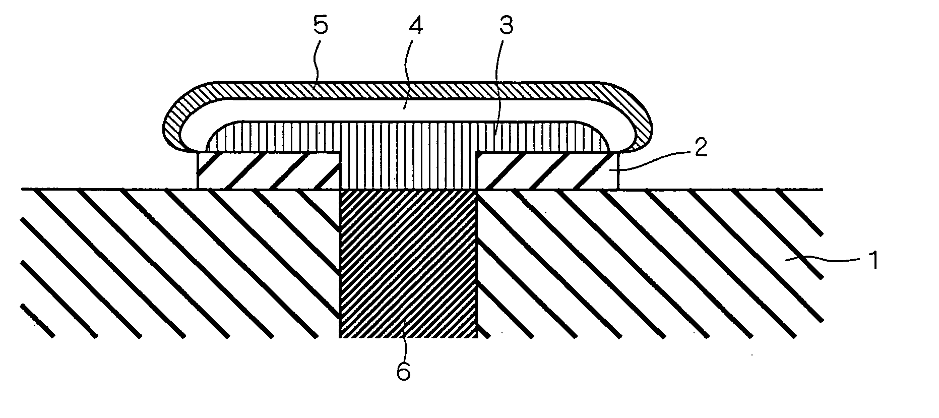
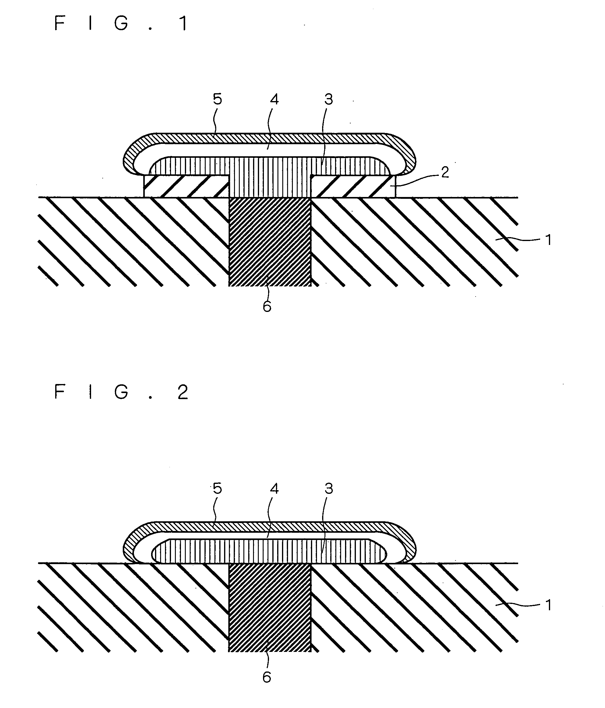
[0024]FIG. 1 is a sectional view showing a structure of a glass ceramic substrate in accordance with the first preferred embodiment. More specifically, FIG. 1 is an enlarged sectional view showing a conductive portion 3 on which plating films 4 and 5 are formed and its vicinity.

[0025] As shown in FIG. 1, the glass ceramic substrate is a complex consisting of a base 1 formed of glass and ceramic (e.g., alumina and aluminum nitride, or the like), an intermediate layer 2, a conductive portion 3 and plating films 4 and 5.

[0026] Specifically, the intermediate layer 2 is formed into a convex shape on a main surface of the base 1. On the intermediate layer 2, the conductive portion 3 is formed. A nickel-plating film 4 and a gold-plating film 5 are formed on the conductive portion 3 in this order, covering the co...


PUM

PropertyMeasurementUnit
thicknessaaaaaaaaaa
thicknessaaaaaaaaaa
diameteraaaaaaaaaa

Abstract

A substrate has a base, an intermediate layer a conductive layer, and conductive films. The base is a ceramic insulator. The intermediate layer on a main surface of the base. The conductive layer is on the intermediate layer The conductive films are on the conductive layer, covering an exposed portion of the conductive layer.

Description

BACKGROUND OF THE INVENTION [0001] 1. Field of the Invention [0002] The present invention relates to a substrate having an insulating base and can be applied to, for example, a substrate having a ceramic or glass ceramic base. [0003] 2. Description of the Background Art [0004] In wide-raging areas of technology such as information network, ceramic substrates and glass ceramic substrates are heavily used. [0005] A ceramic substrate is a complex consisting of a ceramic base, a conductive portion, a plating film and the like. The conductive portion is formed on the ceramic base and the plating film is so formed as to cover the conductive portion. When the ceramic substrate having the above structure is manufactured, there is a case where part of the plating film is joined to an upper surface of the ceramic base. [0006] When the ceramic substrate having the above structure is thermally treated with temperature changes, there is a case where cracks appear on the upper surface of the cera...

Claims


Application Information

Patent Timeline
Patent Type & Authority Applications(United States)
IPC IPC(8): B32B7/02C04B35/10C04B35/14C04B35/185C04B35/581C04B35/584H01L23/13H01L23/15H01L23/498H01L23/538H05K1/03H05K1/11H05K3/24H05K3/40
CPCH01L23/13Y10T428/24926H01L23/49822H01L23/538H01L23/5383H01L2924/09701H05K1/0306H05K1/113H05K3/246H05K3/4061H05K2201/0175H05K2201/0347H05K2201/09045H05K2201/09436H05K2203/0594H01L2924/0002H01L23/498H01L2924/00
Inventor YAMADA, AKIRANOZAKI, AYUMIYAMASHITA, SHU
Owner MITSUBISHI ELECTRIC CORP
Learn More