
Semiconductor component having at least one organic semiconductor layer and method for fabricating the same

a technology of organic semiconductor and semiconductor layer, which is applied in the direction of solid-state devices, coatings, chemical vapor deposition coatings, etc., can solve the problems of inability to produce circuits that are able to function correctly, difficult to design integrated circuits based on organic transistors, and limited options for providing organic semiconductor layers with a protective layer that protects the semiconductor layers from environmental influences, in particular moisture, to achieve the effect of low cost and high resistance to moistur

Inactive Publication Date: 2005-09-08
POLARIS INNOVATIONS LTD
View PDF7 Cites 9 Cited by
  • Summary
  • Abstract
  • Description
  • Claims
  • Application Information

AI Technical Summary

Benefits of technology

[0010] After the treatment with this system, the same disadvantageous effects are observed (shift in the threshold voltage, deterioration in the subthreshold swing, reduction in the on / off ratio and increase in the hysteresis of the transistors) as occur under the action of moisture on a comparable, untreated substrate over the course of time.
[0011] The aspect of the invention provides an apparatus and a method that is highly resistant to moisture or with which a corresponding apparatus can be fabricated.
[0012] According to the preferred embodiment of the invention, this aspect is achieved by a semiconductor component having at least one protective layer for at least partially covering the at least one organic semiconductor layer to protect against environmental influences, the at least one protective layer containing a proportion of an alkane with CnH2n+1 and n greater than or equal to 15 or consisting entirely of an alkane of this type or of a mixture of alkanes of this type, in particular a paraffin wax.
[0013] Alkanes and paraffin wax are inexpensive and can be vaporized without decomposing even at relatively low temperatures. Therefore, a paraffin layer can be applied at low cost. The film of paraffin that has been deposited on the surface of the active organic layer (organic semiconductor layer) not only offers virtually one hundred percent protection against atmospheric humidity (diffusion barrier) but also provides protection against direct contact with water and all solvents that do not attack and / or diffuse through the paraffin layer, and therefore also allows subsequent processes to be carried out on the organic active layer protected in this way, for example subsequent patterning of the organic layer using the aqueous PVA / ADC system, without altering the original properties of the component.
[0014] In this context, it is advantageous if at least one protective layer is between 50 nm and 5 μm thick.
[0015] For further processing, it is advantageous if a polyvinyl alcohol layer is arranged on at least one protective layer as an etching mask.

Problems solved by technology

These effects make it difficult to design integrated circuits based on organic transistors or make it altogether impossible to produce circuits that are able to function correctly.
The possible options for providing organic semiconductor layers with a protective layer that protects the semiconductor layers from environmental influences, in particular, moisture, are limited.
After the treatment with this system, the same disadvantageous effects are observed (shift in the threshold voltage, deterioration in the subthreshold swing, reduction in the on / off ratio and increase in the hysteresis of the transistors) as occur under the action of moisture on a comparable, untreated substrate over the course of time.

Method used


Image

  • Semiconductor component having at least one organic semiconductor layer and method for fabricating the same
  • Semiconductor component having at least one organic semiconductor layer and method for fabricating the same
  • Semiconductor component having at least one organic semiconductor layer and method for fabricating the same

Examples


example 1

Application of a Protective Paraffin Layer from the Vapor Phase.

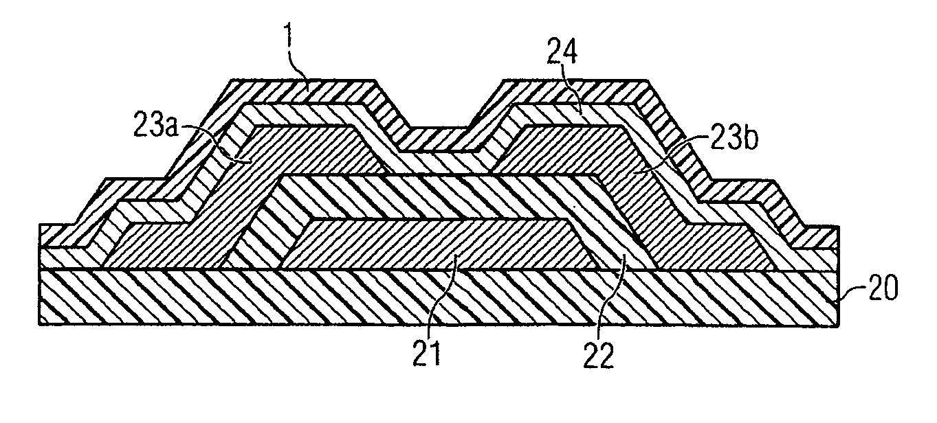
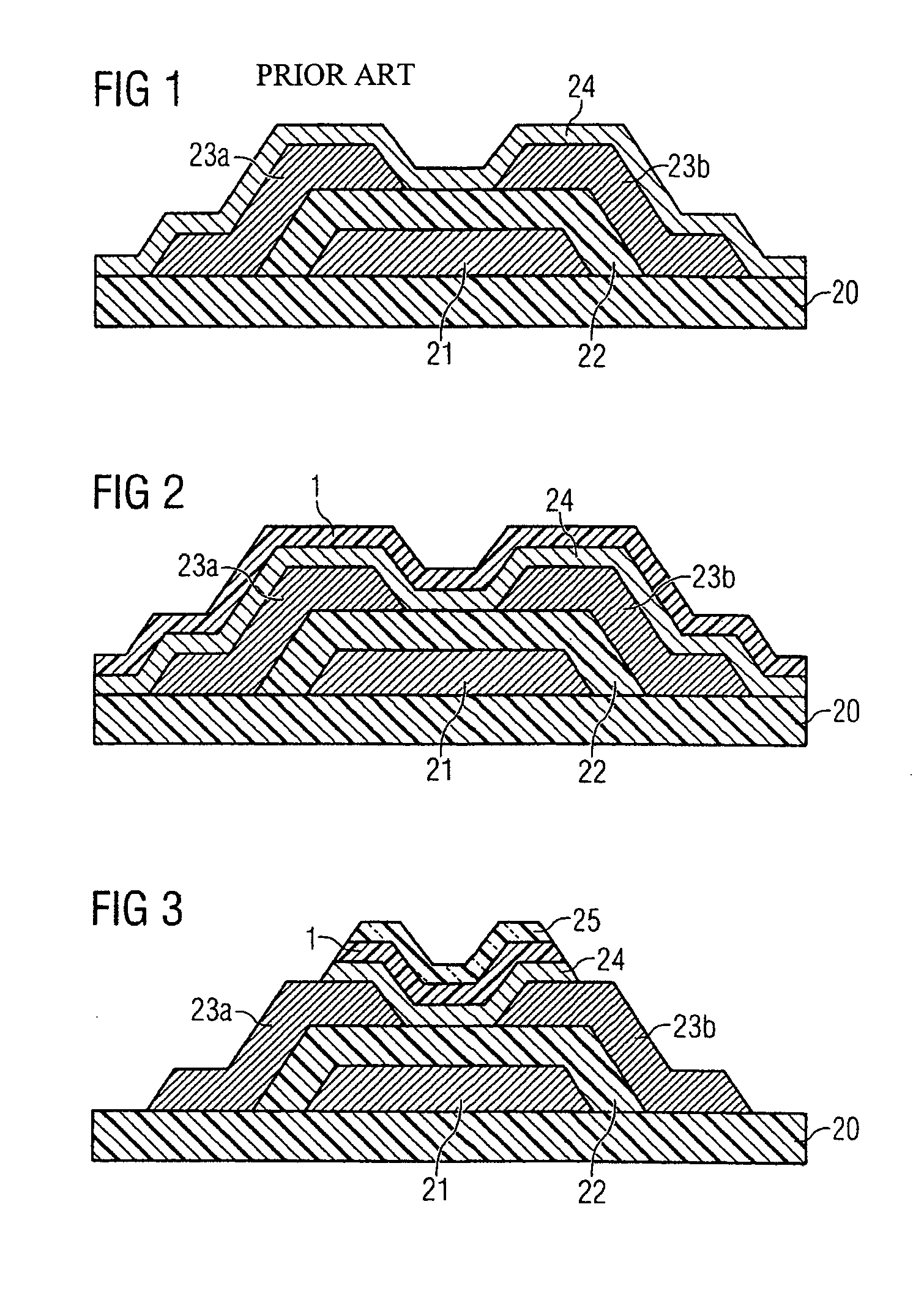
[0056] A freshly produced semiconductor component (transistors and integrated circuits based on organic semiconductors on any desired substrates), in which an organic semiconductor layer 24 (e.g., pentacene) was deposited in the last process step (see for example, FIG. 1) is introduced into a vacuum vaporizer with substrate cooling. The temperature of the substrate holder is controlled to 25-50° C. (preferably 25° C.). Depending on the substrate size, the vaporizer source is loaded with a maximum of 1 g of paraffin wax (solidification point 73-80° C.—Aldrich) and then evacuated. The source is heated at a pressure of 10−2 to 10−4 torr (preferably 10−3 torr). The paraffin sublimes at a temperature of at most 200° C. (preferably 120 to 150° C.) and is deposited as a protective layer 1 on the cooled substrate. The layer thickness of the protective layer 1 can be set by means of the duration of vaporization (preferably 50 n...

example 2

Subsequent Processes Carried out on the Protective Paraffin Layer (Patterning of the Organic Semiconductor Layer).

[0057] A semiconductor component is provided with a protective layer 1 of paraffin in the same way as in Example 1. Then, an aqueous PVA / ADC formulation (see the article by Sheraw et al., cited above and incorporated herein by reference) is spun on (see FIG. 3, PVA layer 25), exposed using a photomask and developed in water. Then, the paraffin layer and the organic semiconductor layer 24 are etched in an oxygen plasma, with the UV-cured PVA layer 25 serving as an etching mask. Alternatively, the PVA etching mask can be printed onto the paraffin layer and cured by floodlight exposure.

example 3

Reducing the Influence of Moisture on the Subthreshold Swing and the On / Off Ratio

[0058] The effect of the exemplary embodiments according to the invention is demonstrated on the basis of measured values.

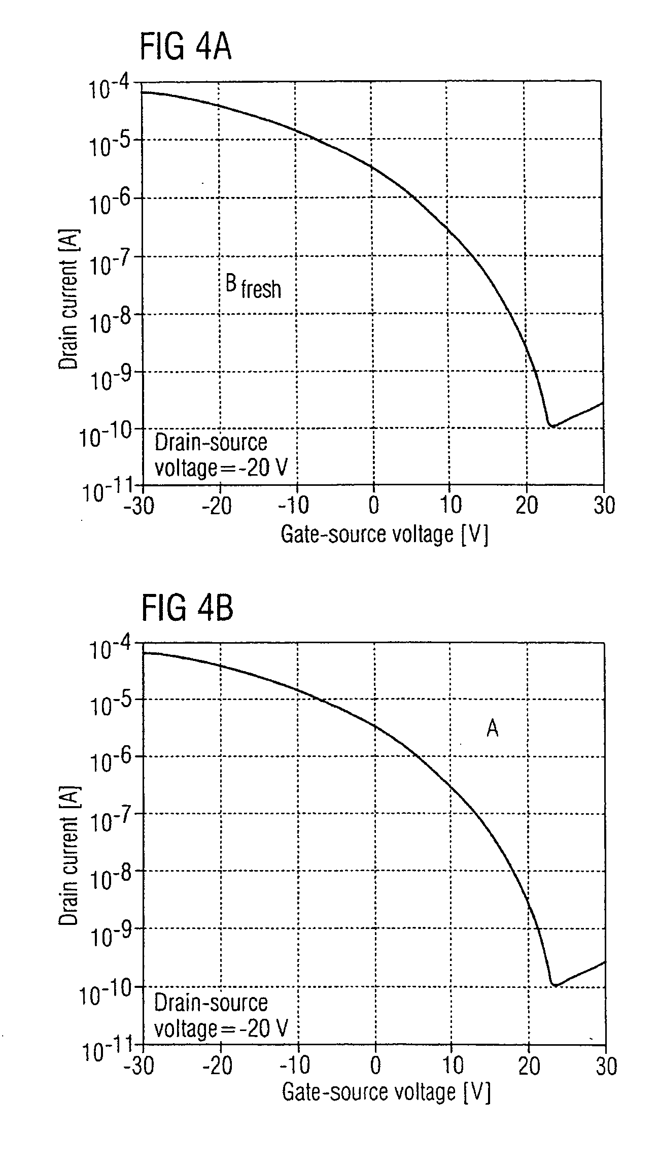
[0059] Two substrates (of which substrate A was coated with a protective layer 1 comprising paraffin as described in Example 1 and substrate B was left untreated) were stored for 10 days under 75% atmospheric humidity. The substrates were measured electrically before (e.g., FIG. 4A for Bfresh) and after storage (FIG. 4B for A and FIG. 4C for B). The drain current is in each case plotted against the gate-source voltage for a given drain-source voltage. The subthreshold swing and the on / off ratio of the transistors can be determined from this curve. Whereas, with substrate B a considerable deterioration was observed as a result of the action of moisture, the characteristic curve of substrate A remained virtually unchanged.


PUM

PropertyMeasurementUnit
thickaaaaaaaaaa
thickaaaaaaaaaa
temperatureaaaaaaaaaa

Abstract

A semiconductor component has at least one organic semiconductor layer. The component also includes at least one protective layer for at least partially covering the at least one organic semiconductor layer to protect against environmental influences. The at least one protective layer contains a proportion of an alkane with CnH2n+1 and n greater than or equal to 15 or consists entirely of an alkane of this type, or of a mixture of alkanes of this type. In one example, the protective layer is a paraffin wax. This creates a high resistance to moisture.

Description

[0001] This application claims priority to German Patent Application 102004010094.2, which was filed Feb. 27, 2004, and is incorporated herein by reference. TECHNICAL FIELD [0002] The invention relates to a semiconductor component having at least one organic semiconductor layer and to a method for fabricating the same. BACKGROUND [0003] A more or less long service life of the electric circuits, depending on the particular application, is required for electronic products based on organic field-effect transistors (OFETs) and circuits to be commercially viable. [0004] The best circuit properties are achieved using bottom-contact architecture (see H. Klauk, M. Halik, U. Zschieschang, F. Eder, G. Schmid, and C. Dehm, “Pentacene organic transistors and ring oscillators on glass and on flexible polymeric substrates,”Appl. Phys. Lett., vol. 82, p. 4175 (2003), which is incorporated herein by reference). [0005] It has been found that transistor properties, for example of OFETs produced using...

Claims


Application Information

Patent Timeline
Patent Type & Authority Applications(United States)
IPC IPC(8): C23C16/00H01L21/31H10K99/00
CPCH01L51/107H01L51/0545H10K10/88H10K10/466
Inventor EDER, FLORIANHALIK, MARCUSKLAUK, HAGENSCHMID, GUNTERZSCHIESCHANG, UTE
Owner POLARIS INNOVATIONS LTD
Learn More